


MaxLoader User’s Guide
24
count and turnaround time. PLDs are programmed according to a fuse map,
which is typically contained in a JEDEC file.
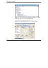
NOTE: PLD compiler CUPL EE Tools offers PLD development tool for
engineers who want to generate a JEDEC file for data of PLD devices. Four
different tools are available in www.eetools.com
PLD Features
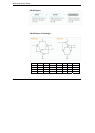
Many different PLDs are available from the IC manufacturers. PLDs are
fabricated using either bipolar or CMOS Processes. All PLDs are made up of
combinations of AND gates, OR gates, inverters, and flip-flops.
PAL
: The PAL is a PLD with a fuse-programmable AND array. The
PAL’s AND gates connect to OR gates in a fixed pattern.
PROM
: For many years, the PROM was not classified as a PLD, even
though most of the smaller PROMs (i.e. 32 x 8 organization) were being used as
logic elements. The larger PROMs were still applied in bipolar microprocessor
designs to store microcode instructions. The PROM has an architecture similar
to the PAL, except that the PROM’s AND array is fixed while it’s OR array is
programmable.
FPLA
: The field-programmable logic array (FPLA) consists of a
programmable AND array like the PAL, with a programmable OR array like the
PROM. The FPLA is therefore a more general PLD because any product term
may be connected to any output OR gate. Because the entire IC is
programmable, the FPLA can implement some functions which a PAL or
PROM may not be able to implement.
EPLD
: Several manufacturers produce PLDs which can be erased and