Interfaces
24 Datasheet, Volume 1
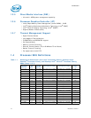
Note:
1. DIMM module support is based on availability and is subject to change.
Note:
1. System memory configurations are based on availability and are subject to change.
2.1.2 System Memory Timing Support
The IMC supports the following Speed Bins, CAS Write Latency (CWL), and command
signal mode timings on the main memory interface:
• tCL = CAS Latency
• tRCD = Activate Command to READ or WRITE Command delay
• tRP = PRECHARGE Command Period
• CWL = CAS Write Latency
• Command Signal modes = 1N indicates a new command may be issued every clock
and 2N indicates a new command may be issued every 2 clocks. Command launch
mode programming depends on the transfer rate and memory configuration.
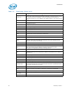
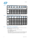
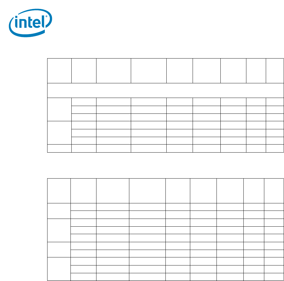
Table 2-2. Supported UDIMM Module Configurations
Raw
Card
Version
DIMM
Capacity
DRAM
Device
Technology
DRAM
Organization
# of
DRAM
Devices
# of
Physical
Device
Ranks
# of
Row/Col
Address
Bits
# of
Banks
Inside
DRAM
Page
Size
Desktop Platforms:
Unbuffered/Non-ECC Supported DIMM Module Configurations
A
1 GB 1 Gb 128 M X 8 8 1 14/10 8 8K
2 GB 2 Gb 128 M X 16 8 1 1510 8 8K
4 GB 4 Gb 512 M X 8 8 1 15/10 8 8K
B
2 GB 1 Gb 128 M X 8 16 2 14/10 8 8K
4 GB 2 Gb 256 M X 8 16 2 15/10 8 8K
8 GB 4 Gb 512 M X 8 16 2 16/10 8 8K
C 1 GB 2 Gb 128 M X 16 4 1 14/10 8 16K
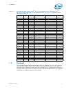
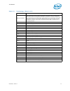
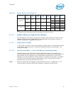
Table 2-3. Supported SO-DIMM Module Configurations (AIO Only)
Raw
Card
Version
DIMM
Capacity
DRAM
Device
Technology
DRAM
Organization
# of
DRAM
Devices
# of
Physical
Device
Ranks
# of
Row/Col
Address
Bits
# of
Banks
Inside
DRAM
Page
Size
A
2 GB 2 Gb 128 M x 16 8 2 14/10 8 8K
4 GB 4 Gb 256 M x 16 8 2 15/10 8 8K
B
1 GB 1 Gb 128 M x 8 8 1 14/10 8 8K
2 GB 2 Gb 256 M x 8 8 1 15/10 8 8K
4 GB 4 Gb 512 M x 8 8 1 16/10 8 8K
C
1 GB 2 Gb 128 M x 16 4 1 14/10 8 8K
2 GB 4 Gb 256 M x 16 4 1 15/10 8 8K
F
2 GB 1 Gb 128 M x 8 16 2 14/10 8 8K
4 GB 2 Gb 256 M x 8 16 2 15/10 8 8K
8 GB 4 Gb 512 M x 8 16 2 16/ 10 8 8K


