Datasheet, Volume 1 91
Electrical Specifications
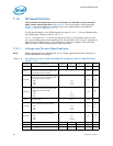
7.11.2 DC Characteristics
The PECI interface operates at a nominal voltage set by V
CCIO
. The DC electrical
specifications shown in Table 7-10 are used with devices normally operating from a
V
CCIO
interface supply. V
CCIO
nominal levels will vary between processor families. All
PECI devices will operate at the V
CCIO
level determined by the processor installed in the
system. For specific nominal V
CCIO
levels, refer to Table 7-5.
Notes:
1. V
CCIO
supplies the PECI interface. PECI behavior does not affect V
CCIO
min/max specifications.
2. The leakage specification applies to powered devices on the PECI bus.
3. The PECI buffer internal pull up resistance measured at 0.75*V
CCIO.
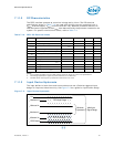
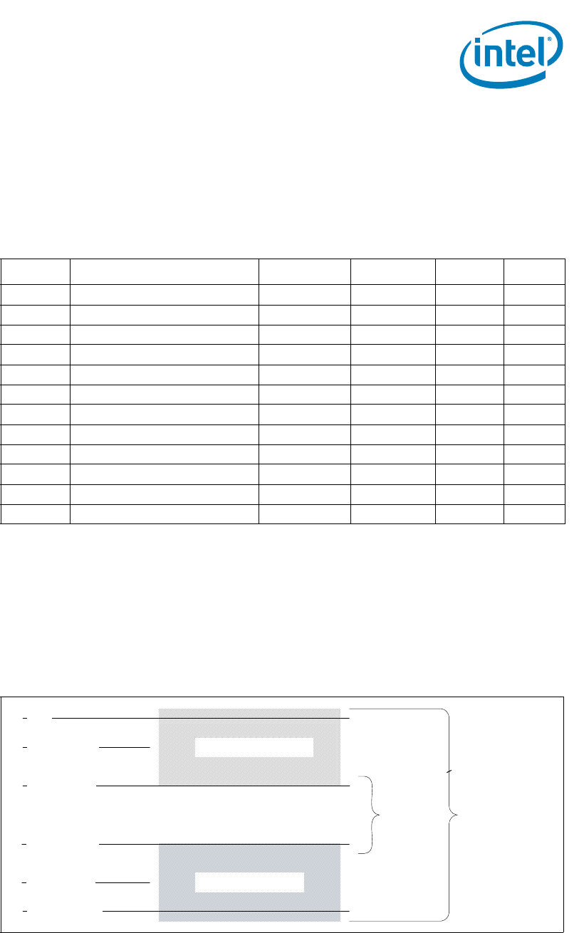
7.11.3 Input Device Hysteresis
The input buffers in both client and host models must use a Schmitt-triggered input
design for improved noise immunity. Use Figure 7-2 as a guide for input buffer design.
§ §
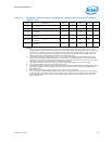
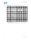
Table 7-10. PECI DC Electrical Limits
Symbol Definition and Conditions Min Max Units Notes
1
Rup
Output resistance 15 45 3
V
in
Input Voltage Range -0.15 V
CCIO
V
V
hysteresis
Hysteresis 0.1 * V
CCIO
N/A V
V
n
Negative-Edge Threshold Voltage 0.275 * V
CCIO
0.500 * V
CCIO
V
V
p
Positive-Edge Threshold Voltage 0.550 * V
CCIO
0.725 * V
CCIO
V
C
bus
Bus Capacitance per Node N/A 10 pF
Cpad
Pad Capacitance 0.7 1.8 pF
Ileak000 leakage current at 0V — 0.6 mA
Ileak025 leakage current at 0.25*V
CCIO
—0.4mA
Ileak050 leakage current at 0.50*V
CCIO
—0.2mA
Ileak075 leakage current at 0.75*V
CCIO
—0.13mA
Ileak100 leakage current at V
CCIO
—0.10mA
Figure 7-2. Input Device Hysteresis
Minimum V
P
Maximum V
P
Minimum V
N
Maximum V
N
PECI High Range
PECI Low Range
Valid Input
Signal Range
Minimum
Hysteresis
V
TTD
PECI Ground


