Electrical Specifications
76 Datasheet, Volume 1
7.3 Processor Clocking (BCLK[0], BCLK#[0])
The processor uses a differential clock to generate the processor core operating
frequency, memory controller frequency, system agent frequencies, and other internal
clocks. The processor core frequency is determined by multiplying the processor core
ratio by the BCLK frequency. Clock multiplying within the processor is provided by an
internal phase locked loop (PLL) that requires a constant frequency input, with
exceptions for Spread Spectrum Clocking (SSC).
The processor’s maximum non-turbo core frequency is configured during power-on
reset by using its manufacturing default value. This value is the highest non-turbo core
multiplier at which the processor can operate. If lower maximum speeds are desired,
the appropriate ratio can be configured using the FLEX_RATIO MSR.
7.3.1 Phase Lock Loop (PLL) Power Supply
An on-die PLL filter solution is implemented on the processor. Refer to Table 7-5 for DC
specifications.
7.4 V
CC
Voltage Identification (VID)
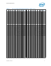
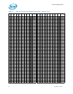
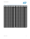
The processor uses three signals for the serial voltage identification interface to support
automatic selection of voltages. Table 7-1 specifies the voltage level corresponding to
the eight bit VID value transmitted over serial VID. A ‘1’ in this table refers to a high
voltage level and a ‘0’ refers to a low voltage level. If the voltage regulation circuit
cannot supply the voltage that is requested, the voltage regulator must disable itself.
VID signals are CMOS push/pull drivers. Refer to Table 7-8 for the DC specifications for
these signals. The VID codes will change due to temperature and/or current load
changes to minimize the power of the part. A voltage range is provided in Table 7-4.
The specifications are set so that one voltage regulator can operate with all supported
frequencies.
Individual processor VID values may be set during manufacturing so that two devices
at the same core frequency may have different default VID settings. This is shown in
the VID range values in Table 7-4. The processor
provides the ability to operate while
transitioning to an adjacent VID and its associated voltage. This will represent a DC
shift in the loadline.
Note: At condition outside functional operation condition limits, neither functionality nor long
term reliability can be expected. If a device is returned to conditions within functional
operation limits after having been subjected to conditions outside these limits, but
within the absolute maximum and minimum ratings, the device may be functional, but
with its lifetime degraded on exposure to conditions exceeding the functional operation
condition limits.


