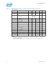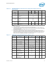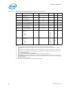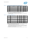
Electrical Specifications
82 Datasheet, Volume 1
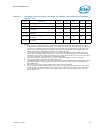
Notes:
1. Refer to Chapter 8 for signal description details.
2. SA and SB refer to DDR3 Channel A and DDR3 Channel B.
3. The maximum rise/fall time of UNCOREPWRGOOD is 20 ns.
4. PE_TX[3:0]/PE_TX#[3:0] and PE_RX[3:0]/PE_RX#[3:0] signals are only used for platforms that support
20 PCIe* lanes. These signals are reserved on Desktop 3rd Generation Intel Core™ i7/i5 processors.
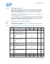
Note: All Control Sideband Asynchronous signals are required to be asserted/de-asserted for
at least 10 BCLKs with maximum T
rise
/T
fall
of 6 ns in order for the processor to
recognize the proper signal state. See
Section 7.10 for the DC specifications.
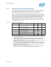
7.8 Test Access Port (TAP) Connection
Due to the voltage levels supported by other components in the Test Access Port (TAP)
logic, Intel recommends the processor be first in the TAP chain, followed by any other
components within the system. A translation buffer should be used to connect to the
rest of the chain unless one of the other components is capable of accepting an input of
the appropriate voltage. Two copies of each signal may be required with each driving a
different voltage level.
The processor supports Boundary Scan (JTAG) IEEE 1149.1-2001 and IEEE 1149.6-
2003 standards. A small portion of the I/O lands may support only one of those
standards.
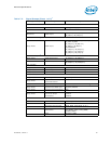
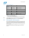
PCI Express*
Differential PCI Express Input
PEG_RX[15:0], PEG_RX#[15:0],
PE_RX[3:0]
4
, PE_RX#[3:0]
4
Differential PCI Express Output
PEG_TX[15:0], PEG_TX#[15:0],
PE_TX[3:0]
4
, PE_TX#[3:0]
4
Single Ended Analog Input PEG_ICOMP0, PEG_COMPI, PEG_RCOMP0
DMI
Differential DMI Input DMI_RX[3:0], DMI_RX#[3:0]
Differential DMI Output DMI_TX[3:0], DMI_TX#[3:0]
Intel
®
FDI
Single Ended FDI Input FDI_FSYNC[1:0], FDI_LSYNC[1:0], FDI_INT
Differential FDI Output FDI_TX[7:0], FDI_TX#[7:0]
Single Ended Analog Input FDI_COMPIO, FDI_ICOMPO
Table 7-2. Signal Groups (Sheet 2 of 2)
1
Signal Group Type Signals


