


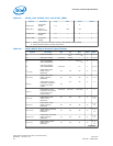
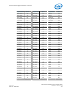
Symbol Definition and Conditions Min Max Units Notes
1
V
n
Negative-Edge Threshold
Voltage
0.275 *
V
CCIO_TERM
0.500
* V
CCIO_TERM
V —
V
p
Positive-Edge Threshold
Voltage
0.550 *
V
CCIO_TERM
0.725 *
V
CCIO_TERM
V —
C
bus
Bus Capacitance per Node N/A 10 pF —
C
pad
Pad Capacitance 0.7 1.8 pF —
Ileak000 leakage current at 0 V — 0.6 mA —
Ileak025 leakage current at 0.25*
V
CCIO_TERM
— 0.4 mA —
Ileak050 leakage current at 0.50*
V
CCIO_TERM
— 0.2 mA —
Ileak075 leakage current at 0.75*
V
CCIO_TERM
— 0.13 mA —
Ileak100 leakage current at
V
CCIO_TERM
— 0.10 mA —
Notes: 1. V
CCIO_TERM
supplies the PECI interface. PECI behavior does not affect V
CCIO_TERM
minimum /
maximum specifications.
2. The leakage specification applies to powered devices on the PECI bus.
3. The PECI buffer internal pull-up resistance measured at 0.75* V
CCIO_TERM
.
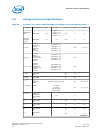
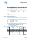
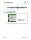
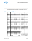
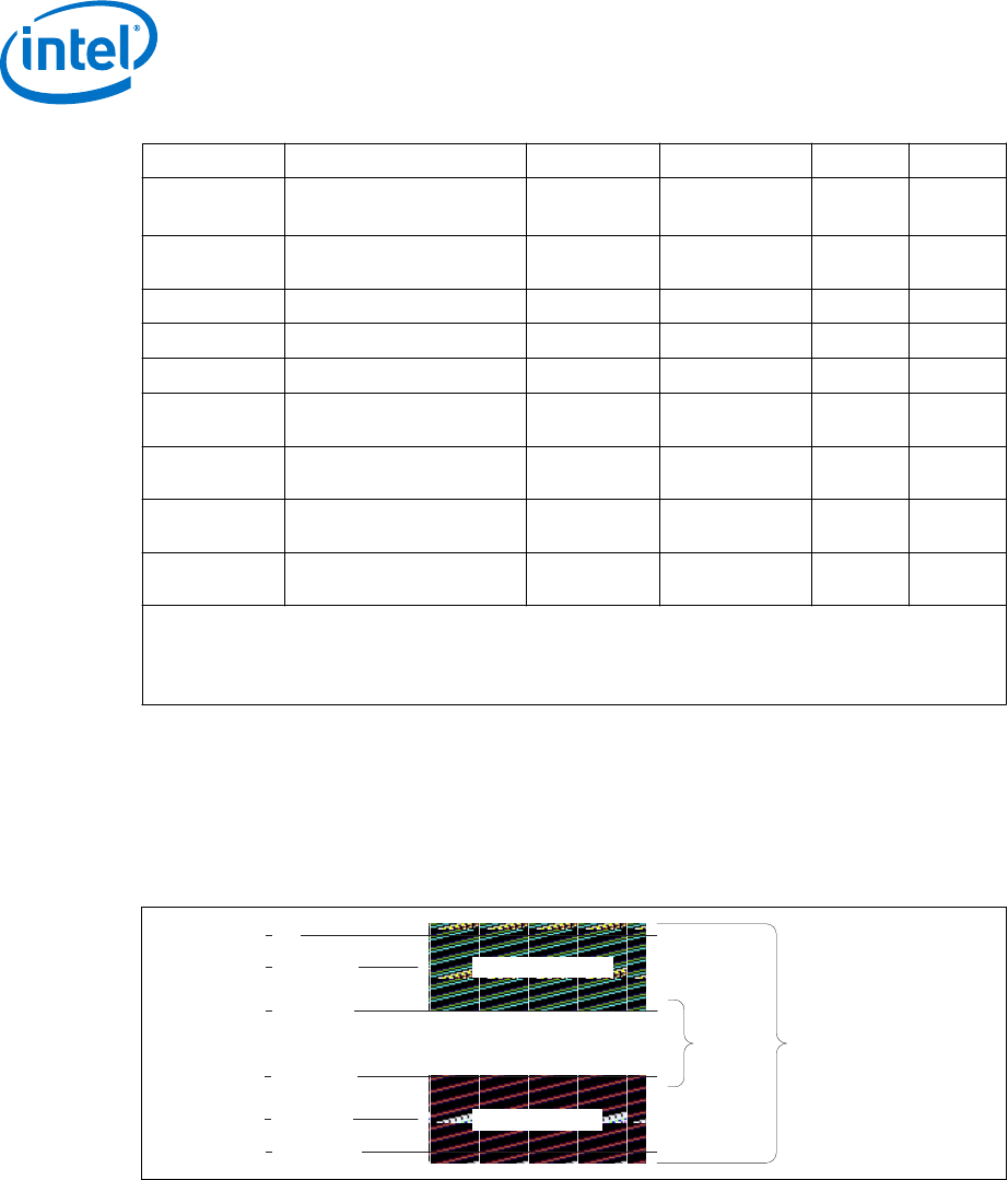
7.8.2 Input Device Hysteresis
The input buffers in both client and host models must use a Schmitt-triggered input
design for improved noise immunity. Use the following figure as a guide for input
buffer design.
Figure 19. Input Device Hysteresis
Minimum V
P
Maximum V
P
Minimum V
N
Maximum V
N
PECI High Range
PECI Low Range
Valid Input
Signal Range
Minimum
Hysteresis
V
TTD
PECI Ground
Processor—Electrical Specifications
Intel
®
Xeon
®
Processor E3-1200 v3 Product Family
Datasheet – Volume 1 of 2 June 2013
100 Order No.: 328907-001