


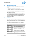
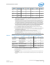
Symbol Parameter Min Max Units Notes
1
V
IH
Input High Voltage (other GTL) V
CCIO_TERM
* 0.72 — V 2, 4
R
ON
Buffer on Resistance (CFG/BPM) 16 24 Ω —
R
ON
Buffer on Resistance (other GTL) 12 28 Ω —
I
LI
Input Leakage Current — ±150 μA 3
Notes: 1. Unless otherwise noted, all specifications in this table apply to all processor frequencies.
2. The V
CCIO_OUT
referred to in these specifications refers to instantaneous VCCIO_OUT.
3. For VIN between 0 V and V
CCIO_TERM
. Measured when the driver is tri-stated.
4. V
IH
and V
OH
may experience excursions above V
CCIO_TERM
. However, input signal drivers must
comply with the signal quality specifications.
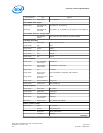
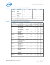
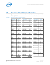
Table 48. PCI Express* DC Specifications
Symbol Parameter Min Typ Max Units Notes
1
Z
TX-DIFF-DC
DC Differential Tx Impedance (Gen 1
Only)
80 — 120 Ω 1, 6
Z
TX-DIFF-DC
DC Differential Tx Impedance (Gen 2 and
Gen 3)
— — 120 Ω 1, 6
Z
RX-DC
DC Common Mode Rx Impedance 40 — 60 Ω 1, 4, 5
Z
RX-DIFF-DC
DC Differential Rx Impedance (Gen1
Only)
80 — 120 Ω 1
PEG_RCOMP Comp Resistance 24.75 25 25.25 Ω 2, 3
Notes: 1. See the PCI Express Base Specification for more details.
2. PEG_RCOMP should be connected to V
COMP_OUT
through a 25 Ω ±1% resistor.
3. Intel allows using 24.9 Ω ±1% resistors.
4. DC impedance limits are needed to ensure Receiver detect.
5. The Rx DC Common Mode Impedance must be present when the Receiver terminations are first
enabled to ensure that the Receiver Detect occurs properly. Compensation of this impedance can
start immediately and the 15 Rx Common Mode Impedance (constrained by RLRX-CM to 50 Ω
±20%) must be within the specified range by the time Detect is entered.
6. Low impedance defined during signaling. Parameter is captured for 5.0 GHz by RLTX-DIFF.
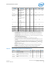
7.8.1 PECI DC Characteristics
The PECI interface operates at a nominal voltage set by V
CCIO_TERM
. The set of DC
electrical specifications shown in the following table is used with devices normally
operating from a V
CCIO_TERM
interface supply.
V
CCIO_TERM
nominal levels will vary between processor families. All PECI devices will
operate at the V
CCIO_TERM
level determined by the processor installed in the system.
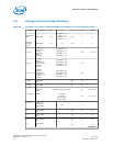
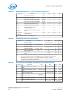
Table 49. PECI DC Electrical Limits
Symbol Definition and Conditions Min Max Units Notes
1
R
up
Internal pull up resistance 15 45 Ω 3
V
in
Input Voltage Range
-0.15
V
CCIO_TERM
+
0.15
V —
V
hysteresis
Hysteresis 0.1 *
V
CCIO_TERM
N/A V —
continued...
Electrical Specifications—Processor
Intel
®
Xeon
®
Processor E3-1200 v3 Product Family
June 2013 Datasheet – Volume 1 of 2
Order No.: 328907-001 99