Theory of Operation
316704-001 / Development Kit User’s Manual 29
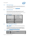
3.4.3 POST Code Debugger
A Port 80-83 Add-in card can be plugged into to the development board at the TPM
header (J9A1). This card decodes the LPC bus BIOS POST codes and displays them on
four 7-segment LED displays.
For AMI* BIOS POST codes, please visit: http://www.ami.com
3.5 Clock Generation
The development board uses a CK-505 and DB800 compatible solution. The FSB
frequency is determined from decoding the processor BSEL[2:0] pin settings.
The clock generator provides Processor, GMCH, ICH8-M, PCI, PCI Express*, SATA, and
USB reference clocks. Clocking for DDR2 is provided by the GMCH.
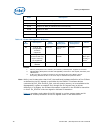
Table 8. Primary System Clocks
Clock Name Speed
CPU 133 MHz @ 533 FSB Speed
166 MHz @ 667 FSB Speed
200 MHz @ 800 FSB Speed
DDR2 133 MHz @ 533 Memory Speed
166 MHz @ 667 Memory Speed
PCI Express* and DMI 100 MHz
SATA 100MHz
PCI 33MHz
USB 48MHz
Super I/O 14MHz
3.6 Power Management States
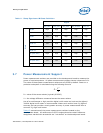
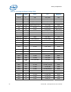
Table 9 and Table 10 lists the power management states that have been defined for
the baseboard.
The Manageability Engine (ME) operates at various power levels, called M-states. M0
is the highest power state, followed by M1 and M-off. The Manageability Engine
provides some of the functionality required to implement Intel
®
Active Management
Technology (iAMT) on the development board. Further information on iAMT can be
found here: http://www.intel.com/technology/manage/iamt/
Table 9. Power Management States
State Description
G0/S0/C0 Full on
G0/S0/C2 STPCLK# signal active


