


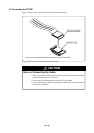
( 32 / 76 )
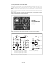
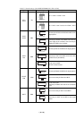
Table 3.2 Switch settings of the M30850T-EPBM (JP1, SW1 to SW4)
Signal Switch Setting Description
VCC1
VCC2
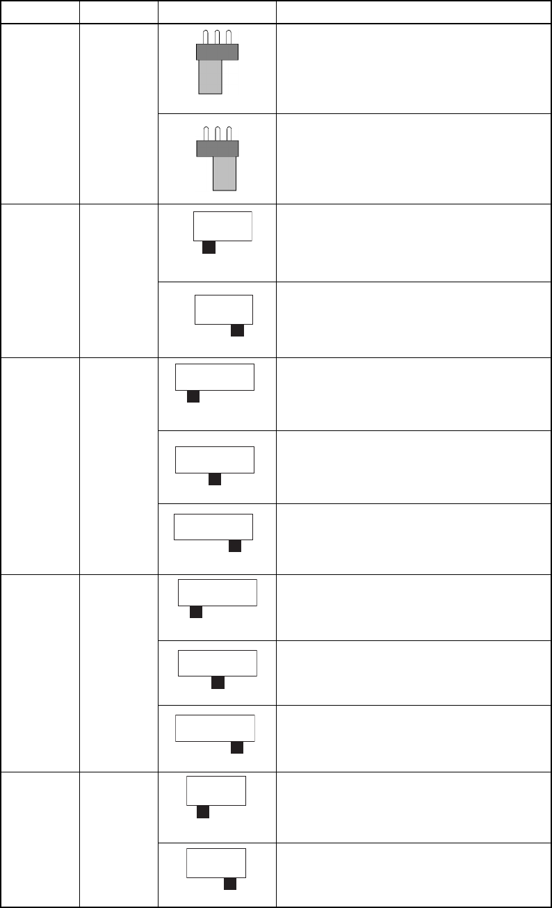
JP1
SW2
XCIN
P87
3.0 V ≤ VCC1 = VCC2 ≤ 5.5 V
4.8 V ≤ VCC1 ≤ 5.2 V and 3.3 V ≤ VCC2 < VCC1
Connects pins AVCC and AVSS of the MCU to the
target system.
Connects pin P87 of the MCU to the target system.
Connects pin AVCC of the MCU to the internal
power supply of the emulator, and connects pin
AVSS to the GND in the emulator.
(Factory-setting)
AVCC
AVSS
SW1
(Factory-setting)
(Factory-setting)
AVCC
AVSS INTEXT
AVCC
AVSS INTEXT
P87 VCONTXCIN
P87 VCONTXCIN
P87 VCONTXCIN
Connects pin P87 of the MCU to the sub-clock
oscillator circuit (32.768 kHz).
Do not set to VCONT.
Pin P87 is disconnected.
XCOUT
P86
SW3
Connects pin P86 of the MCU to the target system.
(Factory-setting)
P86 VSSNC
P86 VSSNC
P86 VSSNC
Does not connect pin P86 of the MCU.
Do not set to VSS.
Connects pin P86 to the VSS in the emulation
probe.
XOUT
SW4
XOU
T
NC
XOUTNC
Connects pin XOUT of the MCU to the target
system.
Does not connect pin XOUT of the MCU.
(Factory-setting)
VCC1=2
VCC1=2
VCC1>2
VCC1>2