


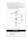
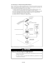

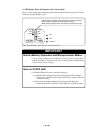
( 52 / 76 )
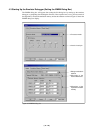
(1) Setting the Debug Monitor Bank Address
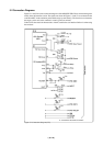
With this product, consecutive 64 KB of the emulator's work area are allocated to the debug monitor.
When "F0" is specified, 64 KB starting from address F00000h are allocated for use by the debug
monitor. Specify an unused area.
IMPORTANT
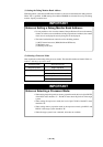
Notes on Setting a Debug Monitor Bank Address:
• It is not possible to view or set the content of the specified area. Even on the memory
window or in the reverse assemble area of the program/source windows, the content
of this area is not displayed correctly though it can be displayed.
• The below bank addresses cannot be set for the debug monitor.
(1) MCU internal resources (ROM, RAM and SFR areas)
(2) Multiplex areas
(3) Interrupt vector area
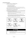
(2) Selecting a Processor Mode
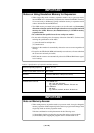
Here explains about the setting of the processor modes. The selectable modes are listed in Table 4.1.
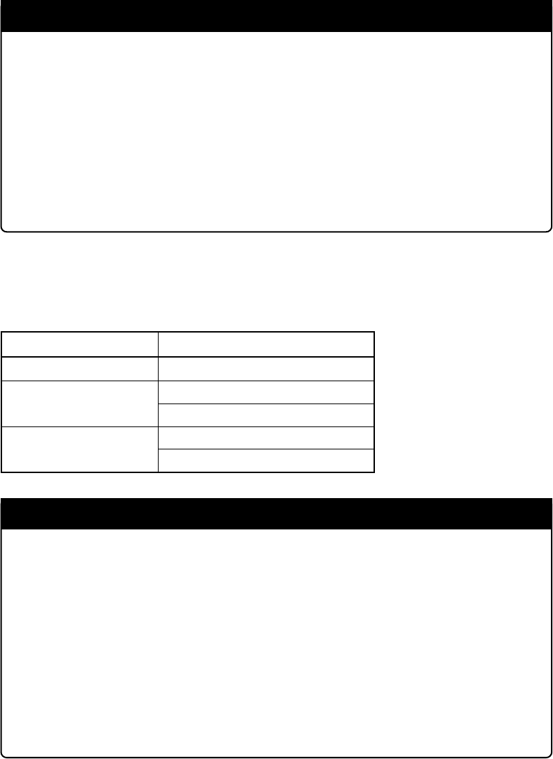
Table 4.1 Selecting a processor mode
IMPORTANT
Notes on Selecting a Processor Mode:
• When setting single-chip mode or memory expansion mode, the level of pin CNVSS
of the MCU status should be "L". The MCU status shows the pin level of the target
system.
•When setting microprocessor mode, the level of pin CNVSS of the MCU status
should be "H".
• When setting memory expansion mode or microprocessor mode, pins RDY* and
HOLD* of the target system should be "H".
•When the target system is not connected, all modes are available.
Processor mode
Single-chip mode
Memory expansion mode
Microprocessor mode
Select from the list
Single-chip Mode
Memory Expansion Mode 8 Bit
Memory Expansion Mode 16 Bit
Microprocessor Mode 8 Bit
Microprocessor Mode 16 Bit