


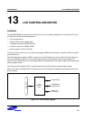
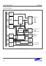

S3C9228/P9228 LCD CONTROLLER/DRIVER
13-3
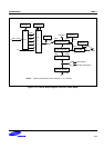
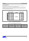
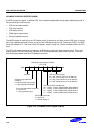
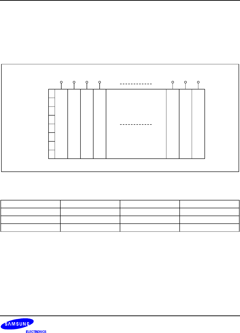
LCD RAM ADDRESS AREA
RAM addresses of page 1 are used as LCD data memory. When the bit value of a display segment is "1", the
LCD display is turned on; when the bit value is "0", the display is turned off.
Display RAM data are sent out through segment pins SEG0–SEG19 using a direct memory access (DMA)
method that is synchronized with the f
LCD
signal. RAM addresses in this location that are not used for LCD
display can be allocated to general-purpose use.
COM0
COM1
COM2
COM3
b0
b1
b2
b3
b4
b5
b6
b7
SEG0
COM7
COM6
COM5
COM4
SEG1 SEG2 SEG3
100H 101H 102H 103H 111H 112H 113H
SEG17 SEG18 SEG19
Figure 13-3. LCD Display Data RAM Organization
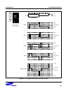
Table 13-1. Common and Segment Pins per Duty Cycle
Duty Common Pins Segment Pins Dot Number
1/8 COM0–COM7 16 pins 128 dots
1/4 COM0–COM3 20 pins 80 dots
1/3 COM0–COM2 20 pins 60 dots