


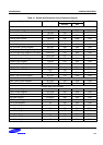

S3C9228/P9228 CONTROL REGISTERS
4-11
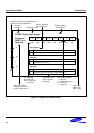
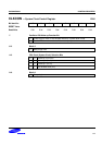
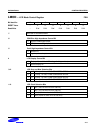
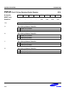
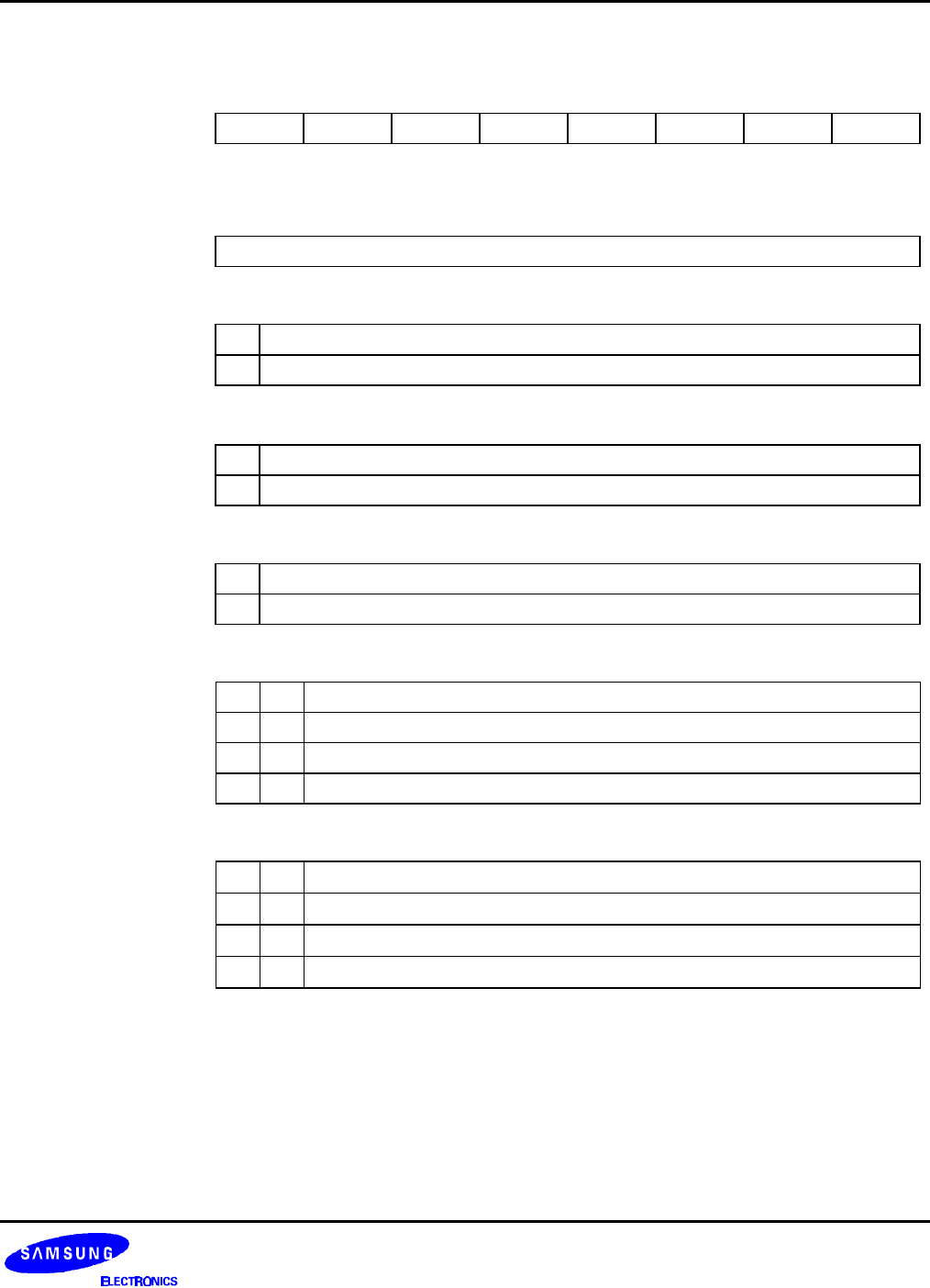
LMOD — LCD Mode Control Register FEH
Bit Identifier .7 .6 .5 .4 .3 .2 .1 .0
RESETRESET Value
– 0 0 0 0 0 0 0
Read/Write
– R/W R/W R/W R/W R/W R/W R/W
.7
Not used for S3C9228/P9228
.6 COM Pins High Impedance Control Bit
0 Normal COMs signal output
1 COM pins are at high impedance
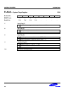
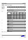
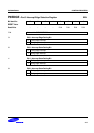
.5 Port3 High Impedance Control Bit
0 Normal I/O
1 High impedance input
.4 LCD Display Control Bit
0
Display off (cut off the LCD voltage dividing resistors)
1
Normal display on
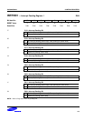
.3-.2 LCD Duty and Bias Selection Bits
0 0 1/3 duty, 1/3 bias; COM0–COM2/SEG0–SEG19
0 1 1/4 duty, 1/3 bias; COM0–COM3/SEG0–SEG19
1 0 1/8 duty, 1/4 bias; COM0–COM7/SEG0–SEG15
1 1 1/8 duty, 1/5 bias; COM0–COM7/SEG0–SEG15
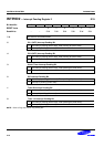
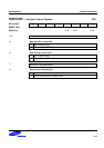
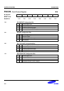
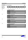
.1-.0 LCD Clock Selection Bits
0 0
fw/2
7
(256 Hz when fw is 32.768 kHz)
0 1
fw/2
6
(512 Hz when fw is 32.768 kHz)
1 0
fw/2
5
(1,024 Hz when fw is 32.768 kHz)
1 1
fw/2
4
(2,048 Hz when fw is 32.768 kHz)