


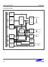

LCD CONTROLLER/DRIVER S3C9228/P9228
13-4
LCD MODE CONTROL REGISTER (LMOD)
A LMOD is located in page 0, at address FEH, and is read/write addressable using register addressing mode. It
has the following control functions.
— LCD duty and bias selection
— LCD clock selection
— LCD display control
— COMs signal output control
— P3 high impedance control
The LMOD register is used to turn the LCD display on/off, to select duty and bias, to select LCD clock, to control
port 3 high impedance/normal I/O port, and to turn the COM signal output on/off. Following a RESET, all LMOD
values are cleared to "0". This turns off the LCD display, select 1/3 duty and 1/3 bias, and select 256Hz for LCD
clock.
The LCD clock signal determines the frequency of COM signal scanning of each segment output. This is also
referred as the LCD frame frequency. Since the LCD clock is generated by watch timer clock (fw). The watch
timer should be enabled when the LCD display is turned on.
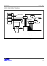
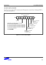
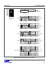
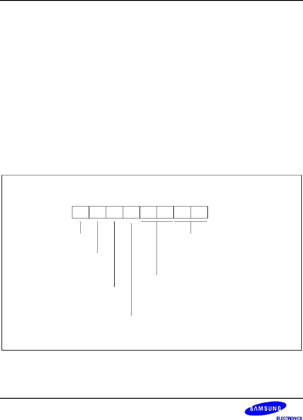
LCD Mode Control Register (LMOD)
FEH, R/W
.7 .6 .5 .4 .3 .2 .1 .0MSB LSB
Not used
LCD duty and bias selection bits:
00 = 1/3 duty, 1/3 bias (COM0-COM2, SEG0-SEG19)
01 = 1/4 duty, 1/3 bias (COM0-COM3, SEG0-SEG19)
10 = 1/8 duty, 1/4 bias (COM0-COM7, SEG0-SEG15)
11 = 1/8 duty, 1/5 bias (COM0-COM7, SEG0-SEG15)
COM pins high impedance
control bit:
0 = Normal COMs signal output
1 = High impendane COM pins
LCD clock selection bits:
00 = fw/2
7
(256 Hz when fw is 32.768 kHz)
01 = fw/2
6
(512 Hz when fw is 32.768 kHz)
10 = fw/2
5
(1024 Hz when fw is 32.768 kHz)
11 = fw/2
4
(2048 Hz when fw is 32.768 kHz)
Port 3 high impendance control bit
0 = Normal I/O
1 = High impendane input
LCD display control bit
0 = Display off
1 = Normal display on
Figure 13-4. LCD Mode Control Register (LMOD)