


1-13 (E)
HDS-X5800
1-8. Input and Output Signals of
Connectors
The input and output signals of the connectors at the rear
panel are as follows.
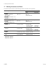
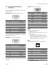
REMOTE2 A/B : RS-422A (D-sub 9-pin, Female)
Pin No. Signal name Input/Output Function
1FG _ Frame ground
2 TX (_) O Transmitted data (_)
3 RX (+) I Received data (+)
4 GND _ Common ground
5 __No connection
6 GND _ Common ground
7 TX (+) O Transmitted data (+)
8 RX (_) I Received data (_)
9 __No connection
The frame ground and the common ground are connected
internally inside the system.
REMOTE3 : RS-232C (D-sub 9-pin, Male)
Pin No. Signal name Input/Output Function
1 DCD I Date carrier detect
2 RX I Received data
3 TX O Transmitted data
4 DTR O Data terminal ready
5 GND _ Signal ground
6 DSR I Date set ready
7 RTS O Request to send
8 CTS I Clear to send
9 __No connection
Pin-6 (DSR) is connected to pin-1 (DCD) internally inside
the system.
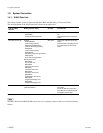
ALARM : D-sub Mini 15-pin, Female
Pin No. Signal name Input/Output Function
1 ALARM-3 O Alarm drive-3
2 ALARM-1 O Alarm drive-1
3 ALARM-4 O Alarm drive-4
4GND _ Ground
5 ALARM-5 O Alarm drive-5
6 to 8 GND _ Ground
9 ALARM-6 O Alarm drive-6
10 GND _ Ground
11 GND _ Ground
12 ALARM-2 O Alarm drive-2
13 to 15 GND _ Ground
n
Specifications of the alarm output
Open collector output
Voltage that can be applied to the terminal : 0 to 20 V
Pull-in current :
Maximum 50 mA when the output transistor is
saturated (output terminal voltage is 1 V or less).
Output terminal voltage x pull-in current < 50 mV
when the output transistor is non-saturated.
DATA :
10BASE-T/100BASE-TX (RJ-45 8-pin Modular jack)
Pin No. Signal name Input/Output Function
1 TDB O Transmitted data B
2 TDA O Transmitted data A
3 RDB I Received data B
4 BI_D3+_ (*1)
5 BI_D3__ (*1)
6 RDA I Received data A
7 BI_D4+_ (*1)
8 BI_D4__ (*1)
*1 : This signal line is not used in this system. It is connected to the
termination circuit inside the system.
_ EXT VIEW _
1
5
69
_ EXT VIEW _
5
1
96
_ EXT VIEW _
1
5
11
15
6
10
1-8. Input and Output Signals of Connectors
1
8
_ EXT VIEW _