12 www.xilinx.com ML310 User Guide
1-800-255-7778 UG068 (v1.01) August 25, 2004
Chapter 1: Introduction to Virtex-II Pro, ISE, and EDK
R
PowerPC™ 405 Core
• Embedded 300+ MHz Harvard architecture core
• Low power consumption: 0.9 mW/MHz
• Five-stage data path pipeline
• Hardware multiply/divide unit
• Thirty-two 32-bit general purpose registers
• 16 KB two-way set-associative instruction cache
• 16 KB two-way set-associative data cache
• Memory Management Unit (MMU)
♦ 64-entry unified Translation Look-aside Buffers (TLB)
♦ Variable page sizes (1 KB to 16 MB)
• Dedicated on-chip memory (OCM) interface
• Supports IBM CoreConnect™ bus architecture
• Debug and trace support
• Timer facilities
RocketIO 3.125 Gb/s Transceivers
• Full-duplex serial transceiver (SERDES) capable of baud rates from 622 Mb/s
to 3.125 Gb/s
• 80 Gb/s duplex data rate (16 channels)
• Monolithic clock synthesis and clock recovery (CDR)
• Fibre Channel, Gigabit Ethernet, 10 Gb Attachment Unit Interface (XAUI), and
Infiniband-compliant transceivers
• 8-, 16-, or 32-bit selectable internal FPGA interface
• 8B /10B encoder and decoder
• 50Ω/75Ω on-chip selectable transmit and receive terminations
• Programmable comma detection
• Channel bonding support (two to sixteen channels)
• Rate matching via insertion/deletion characters
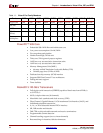
Table 1-1: Virtex-II Pro Family Members
Device 2VP2 2VP4 2VP7 2VP20 2VP30 2VP40 2VP50 2VP70 2VP100 2VP125
Logic Cells 3,168 6,768 11,088 20,880 30,816 43,632 53,136 74,448 99,216 125,136
PPC4050112222224
MGTs 448881216202024
BRAM
(Kbits)
216 504 792 1,584 2,448 3,456 4,176 5,904 7,992 10,008
Xtreme
Multipliers
12 28 44 88 136 192 232 328 444 556


