ML310 User Guide www.xilinx.com 35
UG068 (v1.01) August 25, 2004 1-800-255-7778
Board Hardware
R
CPU Debug Connector Pinout
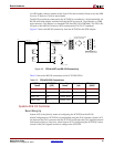
Figure 2-10 shows J12, the 16 pin header used to debug the operation of software in the
CPU. This is done using debug tools such as Parallel Cable IV or third party tools. Refer to
the PPC405 Processor Block Manual for more information on the JTAG debug-port signals.
CPU Debug Connection to XC2VP30
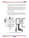
The connection between the CPU debug connector and the XC2VP30 are shown in
Table 2-9. These are attached to the PowerPC™ 405 JTAG debug resources using normal
FPGA routing resources. The JTAG debug resources are not hard-wired to particular pins,
and are available for attachment in the FPGA fabric, making it possible to route these
signals to whichever FPGA pins the user prefers.
PCI Bus
The ML310 board design provides the Xilinx Virtex-II Pro access to two 33MHz/32bit PCI
buses, Primary 3.3V PCI Bus and a Secondary 5.0V PCI Bus. The FPGA is directly
connected to the Primary 3.3V PCI bus while the 5.0V PCI Bus is connected to the Primary
PCI Bus via a PCI-to-PCI Bridge. There are several PCI devices available on the PCI Buses
as well as 4 PCI add-in card Slots. All PCI Bus signals driven by the XC2VP30 comply with
the IO requirements specified in the PCI Local Bus Specification, Revision 2.2.
The majority of the ML310 features are accessed over the 33MHz/32 bit PCI Bus. The
Virtex-II Pro Power PC405 Processors can gain access to the Primary PCI Bus through the
EDK PCI Host Bridge IP. All PCI configuration and control can be performed via a PCI
Host Bridge implemented in the FPAG fabric. The Primary PCI Bus is wired so that the
FPGA fabric must used to provide PCI Bus arbitration logic. The EDK kit also provides PCI
Figure 2-10: CPU Debug Connector (J12)
UG000_05_17_082002
1
216
15
GND
VCC
TRST
HALT_N
TMS
TDO
TDI
TCK
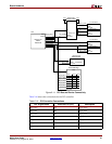
Table 2-9: CPU Debug Connection to XC2VP30
Pin Name XC2VP30 Pin (U37) Connector Pin (J12)
TDO AH19 1
TDI AJ9 3
TRST_N AE12 4
TCK AC13 7
TMS AD13 9
HALT_N AE11 11


