20 www.xilinx.com ML310 User Guide
1-800-255-7778 UG068 (v1.01) August 25, 2004
Chapter 2: ML310 Embedded Development Platform
R
♦ 2 USB ports
♦ 2 IDE connectors
♦ GPIO
♦ SMBus Interface
♦ AC97 Audio CODEC
♦ PS/2 keyboard and mouse ports
• ATX power supply
Board Hardware
The ML310 Virtex-II Pro FPGA is connected to several peripherals listed below. The
peripherals are either directly connected to the FPGA or in directly accessible via the PCI
Bus. The following sections describe the main features of each of the peripherals and how
they interface with the Xilinx Virtex-II Pro. The EDK Processor IP Reference Guide should be
reviewed as well as each of the data sheets corresponding to the devices listed. All device
data sheets are located on the ML310 CDROM.
• DDR DIMM Memory, compatible with EDK supported IP and SW drivers
• FPGA UART, compatible with EDK supported IP and SW drivers
• System ACE, compatible with EDK supported IP and SW drivers
• GPIO- LEDs / LCD, compatible with EDK supported IP and SW drivers
• PCI Bus Interface, compatible with EDK supported IP and SW drivers
♦ ALi M1535D+ PCI Device
♦ Intel Ethernet/NIC PCI Device
• SMBus/IIC, multiple devices available, compatible with EDK supported IP and SW
drivers
♦ LTC1694 SMBUS accelerator
♦ RTC8566 Real time clock
♦ 24LC64 EEPROM 64k bits
♦ LM87 voltage/temp monitor
♦ DDR DIMM SPD EEPROM
• SPI EEPROM, compatible with EDK supported IP and SW drivers
• High speed IO through RocketIO Transceivers
Clock Generation
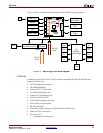
The ML310 board employs a Xilinx XC2VP30-FF896 FPGA. Several clocks are distributed
throughout the ML310 as can be seen in Figure 2-3. The main system clock is a 100 MHz
oscillator, X10. The system clock is typically used to generate multiple clocks with varying
frequency and phases within the FPGA fabric by using the Virtex-II Pro DMCs. The FPGA
also generates and drives clocks required by the DDR DIMM memory and PCI bus
interfaces.
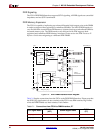
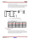
The FPGA requires different banking voltages that are set based on the I/O voltage
interface requirements of each device connected directly to the FPGA. All but two of the
banks are set to 2.5V while banks 1 and 2 are set to 3.0V as shown in Figure 2-3. The Virtex-


