ML310 User Guide www.xilinx.com 27
UG068 (v1.01) August 25, 2004 1-800-255-7778
Board Hardware
R
a UART usable with any member of the Virtex-II Pro device family. Please review the EDK
Processor IP Reference Guide for more details.
The RS-232 port directly connected to the XC2VP30 is accessible by a 10 pin header(J4). An
RS-232 mini-cable adapter included with the ML310 converts J4, 10 pin header, to a DB9
male connector. The adapter is a standard DTK/Intel IDC-10 to DB9 Male. The FPGA RS-
232 port on the ML310 is wired as a DTE and meets the EIA/TIA-574 standard
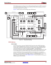
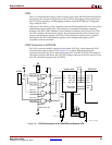
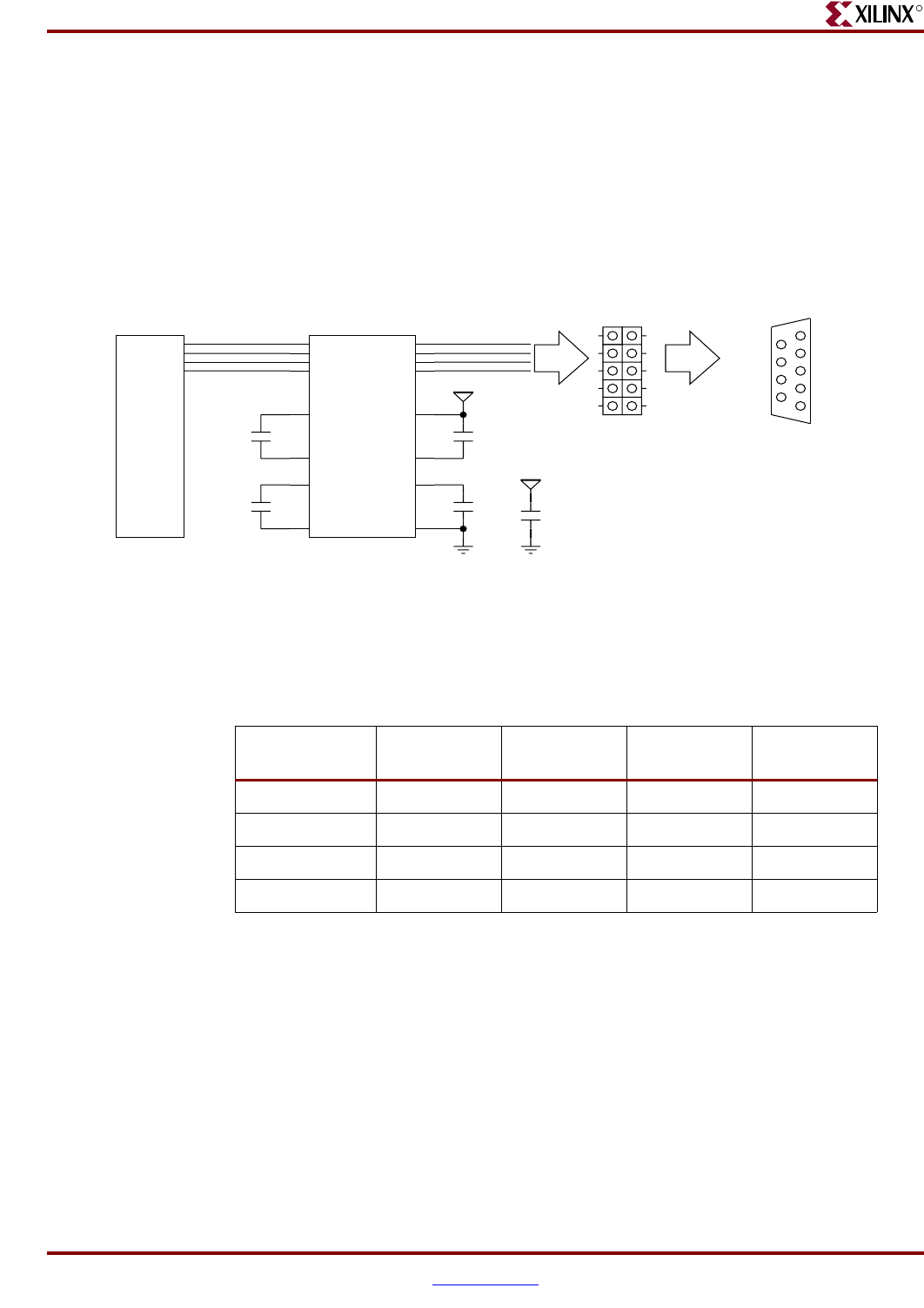
Figure 2-5 shows the RS-232 connectivity from the XC2VP30 to the DTK adapter.
.
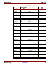
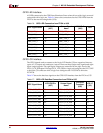
Table 2-3 shows the RS-232 connections to the XCV2VP30 FPGA.
System ACE CF Controller
Board Bring-Up
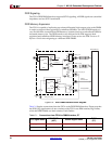
System ACE is the primary means of configuring the XC2VP30 on the ML310
board.Configuration of XC2VP30 is accomplished using the JTAG interface. System ACE
sits between the JTAG connector and the XC2VP30, and passes the JTAG signals back and
forth between the two. However, when System ACE is configuring the XC2VP30, it takes
control of the JTAG signals in order to configure the XC2VP30.
Figure 2-5: FPGA UART and RS-232 Connectivity
UG068_5_32_080204
VCC3V3
VCC3V3
MAX3232
XC2VP30
DIN1
V-C2+
C1-
RIN1
DOUT1
ROUT2
DOUT2
ROUT1
C1+
RIN2
V+
DIN2
VCC
GNDC2-
11
64
3
13
14
9
7
12
1
8
2
10
16
155
U7U37
C327
0.1UF
C331
0.1UF
C330
0.1UF
C326
0.1UF
C313
0.1UF
COM0_CTS
COM0_RXD_N
COM0_RTS
UART0_CTS_N
UART0_RTS_N
UART0_TXD COM0_TXD_N
UART0_RXD
HEADER2X5
RS232 DTE PINOUT
GND
DTR
TX
RX
CD
DSR
RTS
CTS
6
8
9
7
5
4
2
1
3
RI
USE A DTK-PINOUT IDC10
TO DB9 PLUG CABLE.
CONNECTS TO PC WITH
F/F NULL MODEL CABLE.
12
34
56
78
910
J4
Table 2-3: FPGA RS-232 Connections
UCF Signal
Name
XC2VP30 Pin
(U37)
Schem Signal
Name
10 pin Header
(J4)
DTK Adapter
(DB9)
uart1_ctsn B10 UART0_CTS 6 8
uart1_rtsn G14 UART0_RTS 4 7
uart1_sin F14 UART0_RXD 3 2
uart1_sout F12 UART0_TXD 5 3


