54 www.xilinx.com ML310 User Guide
1-800-255-7778 UG068 (v1.01) August 25, 2004
Chapter 2: ML310 Embedded Development Platform
R
CPU Reset, SW2
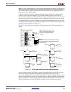
SW2 provides a way to manually reset the powerpc system implemented in the XC2VP30.
The user is responsible for connecting this signal to the PPC405 system implemented in the
FPGA fabric. The EDK kit provides IP to perform this task, please review the EDK Processor
IP reference Guide for more details. When SW2 is actuated it drives the signal
PB_FPGA_CPU_RESET low which causes the LTC1326 (U30) to generate a 100us active
low pulse. The active low output of the LTC1326 pin E16 on the XC2VP30 (U38) device via
signal FPGA_CPU_RESET_N. In addition to resetting the CPU, SW2 can also perform a
System ACE CF reset as described in the above section. This can be accomplished by
simply holding down the SW2 push button for longer than 2 seconds. This action performs
a CPU reset followed by a System ACE CF reset. Please review the ML310 schematics and
the LTC1236 data sheet found on the ML310 CDROM for more details.
The front panel interface header (J23) can also drive the PB_ FPGA_CPU_RESET signal.
For more details on J23, please review section “Front Panel Interface Connector, J23”
System ACE Configuration Dipswitch, SW3
The System ACE configuration dipswitch is a three position dipswitch that controls the
three configuration address pins on the System ACE CF controller. The three configuration
address lines are; CFGADDR0, CFGADDR1 and CFGADDR2 and are marked as positions
1, 2 and 3 respectively on the dipswitch (SW3) plastic housing. Dipswitch SW3 is also
marked with an "on" indicator that is etched onto the plastic housing of SW3 as well as an
arrow head on the board silk-screen for SW3. When any of the three switches are moved to
the "on" position then the associated CFGADDR bit is set to a logic zero. When any of the
three switches are moved opposite of the "on" position then the associated CFGADDR bit
is set to a logic one via a pull-up resistor.
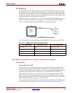
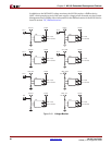
Table 2-16 depicts the SW3 dipswitch connections to the System ACE device. One side of
the dipswitch is tied to pull-ups that are connected to each of the CFGADDR lines while
the other side of the dipswitch is connected to ground. The configuration address lines are
also connected to the Front Panel Interface, see “Front Panel Interface Connector, J23” for
more details. This allows the user to manually select one of eight configurations stored on
the CompactFlash that is connected to the System ACE device. Once the user makes a valid
selection on SW3 the user can then depress push button SW1 to command the System ACE
device to reset and configure the FPGA using the configuration selected by dipswitch SW3.
Please review the System ACE CF data sheet which is available at http://www.xilinx.com
or on the ML310 CDROM.


