ML310 User Guide www.xilinx.com 21
UG068 (v1.01) August 25, 2004 1-800-255-7778
Board Hardware
R
II Pro FPGA I/O can be configured to use different IO standards such as SSTL2 as required
on the DDR DIMM interface. Please review the ML310 Virtex-II Pro data sheet for more
information regarding I/O standards.
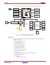
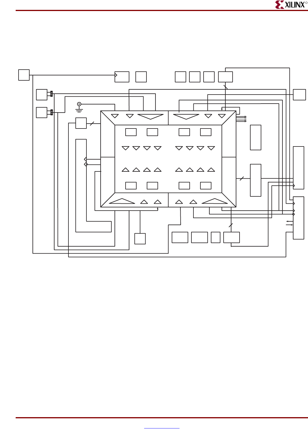
Figure 2-3 shows the top-level clocking for the ML310 board.
DDR Memory
DDR DIMM
The ML310 includes a registered 256MB PC3200 Double Data Rate (DDR) Dual Inline
Memory Module (DIMM) with an industry standard 184-pin count. The DDR DIMM is
commercially available from Wintec Industries as part number W4F232726HA-5Q. The
associated datasheet is provided on the ML310 CDROM. The DDR DIMM is
manufactured using nine Infineon HYB25D256800BT-5, 32Mx8 DDR SDRAM devices with
13-row address lines, 10-column address lines, and 4 bank select lines. Read and write
access to the Infineon devices is programmable in burst lengths of 2, 4, or 8 column
locations. The memory module inputs and outputs are compatible with SSTL2 signaling.
Serial Presence Detect (SPD) using an SMBus interface to the DDR DIMM is also
supported. Please refer to section “IIC/SMBus Interface” for more details on accessing the
DIMM module’s SPD EEPROM.
Figure 2-3: Top-Level Clocking
PM IO
2.5V
LVDS
DDR
DIMM
64 bit
256MB
PM IO
2.5V
LVDS
PCI
BUS
3.0V
DCM
X0Y0
DCM
X1Y0
DCM
X2Y0
DCM
X3Y0
DCM
X0Y1
DCM
X1Y1
DCM
X2Y1
DCM
X03Y1
7S 6P 5S 4P 3S 2P 1S 0P
7P 6S 5P 4S 3P 2S 1P 0S
BANK 0
2.5V
BANK 1
3.0V
BANK 2
3.0V
BANK 3
2.5V
BANK 4
2.5V
BANK 5
2.5V
BANK 6
2.5V
BANK 7
2.5V
LVDS_CLK_LOC_N
LVDS_CLK_LOC_P
USER_CLKSYS
(not used)
DDR_CLK_FB
SYACE_FPGA_CLK
PM_CLK_BOT
LVDS_CLK_EXT_N
LVDS_CLK_EXT_P
LVDS_CLK_LOC_N
LVDS_CLK_LOC_P
LVDS_CLK_EXT_N
LVDS_CLK_EXT_P
PM_CLK_TOP
USER_SMA_CLK
SYS_CLK
(user_clk_pci)
LEDsLCDSYSACE IIC UART
PM IO
3V
CPU
DEBUG
SPITRACE
PM IO
2.5V
12
(6 LVDS)
72
(36 LVDS)
PCI_P_CLK1
thru
PCI_P_CLK4
PCI_P_CLK5
DDR_CLK
DDR_CLKB
DDR_CLK_FB
Note:
All 3 DDR
Clock nets
are length
matched
Note:
All 5 PCI
Clock nets
are length
matched
26
SYACE_FPGA_CLK
OSC
33MHz
J17
X8
OSC
156.25
MHz
OSC
125MHz
J21
J20
X7
X9
PM1
8
MGTs
(to FPGA)
PM2
OSC
100MHz
X10
6
(3 LVDS)
OSC
X6


