26 www.xilinx.com ML310 User Guide
1-800-255-7778 UG068 (v1.01) August 25, 2004
Chapter 2: ML310 Embedded Development Platform
R
unbuffered DIMM requires more than one clock input pair versus a single clock input pair
for a registered DIMM.
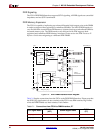
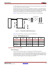
Table 2-2 shows optional clocking connections that are required for interfacing the FPGA
to unbuffered DDR DIMMs.
Serial Port FPGA UART
Introduction to Serial Ports
Serial ports are useful as simple, low-speed interfaces between Data Terminal Equipment
(DTE) such as PCs or terminals and Data Communication Equipment (DCE) such as
modems. A DTE to DCE connection uses a "straight-through" type of cable in which the
transmit (TX) and receive (RX) lines of one end of the cable directly connect to the
corresponding TX and RX wires on the other end of the cable. In a DTE to DTE connection
a "null-modem" type of cable which cross-wires the TX and RX signals from one end of the
cable to the RX and TX signals on the other end is used. Since the ML310 is a DTE, use a
“null modem” cable when connecting to another DTE such as a PC.
Signaling Standards of RS-232
The RS-232 standard specifies output voltage levels between -5 to -15 Volts for logical 1 and
+5 to +15 Volts for logical 0. Inputs must be compatible with voltages in the range of -3V to
-15V for logical 1 and +3V to +15V for logical 0. This ensures data bits are read correctly at
the maximum cable length of 50 feet between two RS-232 connected devices.
Note: A negative voltage represents a logic level 1 while a positive voltage represents a
logic level 0. As these signaling levels are quite high compared to current signaling levels,
transceivers are often used to convert to more manageable levels.
RS-232 on the ML310
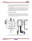
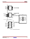
Three RS-232 ports are available on the ML310; two ports (P1) are connected to the ALi
M1535D+ South Bridge (U15) and the third (J4) is connected to the XC2VP30 FPGA (U37)
through a MAX3232 Transceiver (U7).
The two RS-232 ports connected to the ALi South Bridge(U15) are wired such that the
ML310 is a DTE device. These two ports on connector P1 are only accessible by the FPGA
through the PCI Bus. Please review section “ALi South Bridge Interface, M1535D+, U15”
for more information as well as the M1535D+ data sheet
The third RS-232 port is connected directly to the XC2VP30 FPGA and can be accessed by
simply implementing a UART in the FPGA fabric. EDK provides many IP cores, including
Table 2-2: Optional DDR DIMM Clocks for use with Unbuffered DIMMs
Schem Signal XC2VP30 (U37) DIMM (P7)
DDR_CK1 K29 16
DDR_CK1_N L29 17
DDR_CK2 AD30 76
DDR_CK2_N AD25 75
Note:
All 3 DDR differential clock pairs are length matched and controlled impedance.


