ML310 User Guide www.xilinx.com 29
UG068 (v1.01) August 25, 2004 1-800-255-7778
Board Hardware
R
JTAG
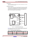
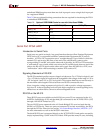
JTAG is a simple interface that provides for many uses. On the ML310 Hardware Platform,
the primary uses include configuration of the XC2VP30, debugging software (similar to
the CPU debug interface), and debugging hardware using the ChipScope™ Integrated
Logic Analyzer (ILA).
The Virtex-II Pro family is fully compliant with the IEEE Standard 1149.1 Test Access Port
and Boundary-Scan Architecture. The architecture includes all mandatory elements
defined in the IEEE 1149.1 Standard. These elements include the Test Access Port (TAP),
the TAP controller, the instruction register, the instruction decoder, the boundary-scan
register, and the bypass register. The Virtex-II Pro family also supports some optional
instructions; the 32-bit identification register, and a configuration register in full
compliance with the standard.
JTAG Connection to XC2VP30
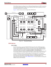
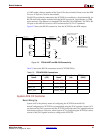
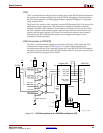
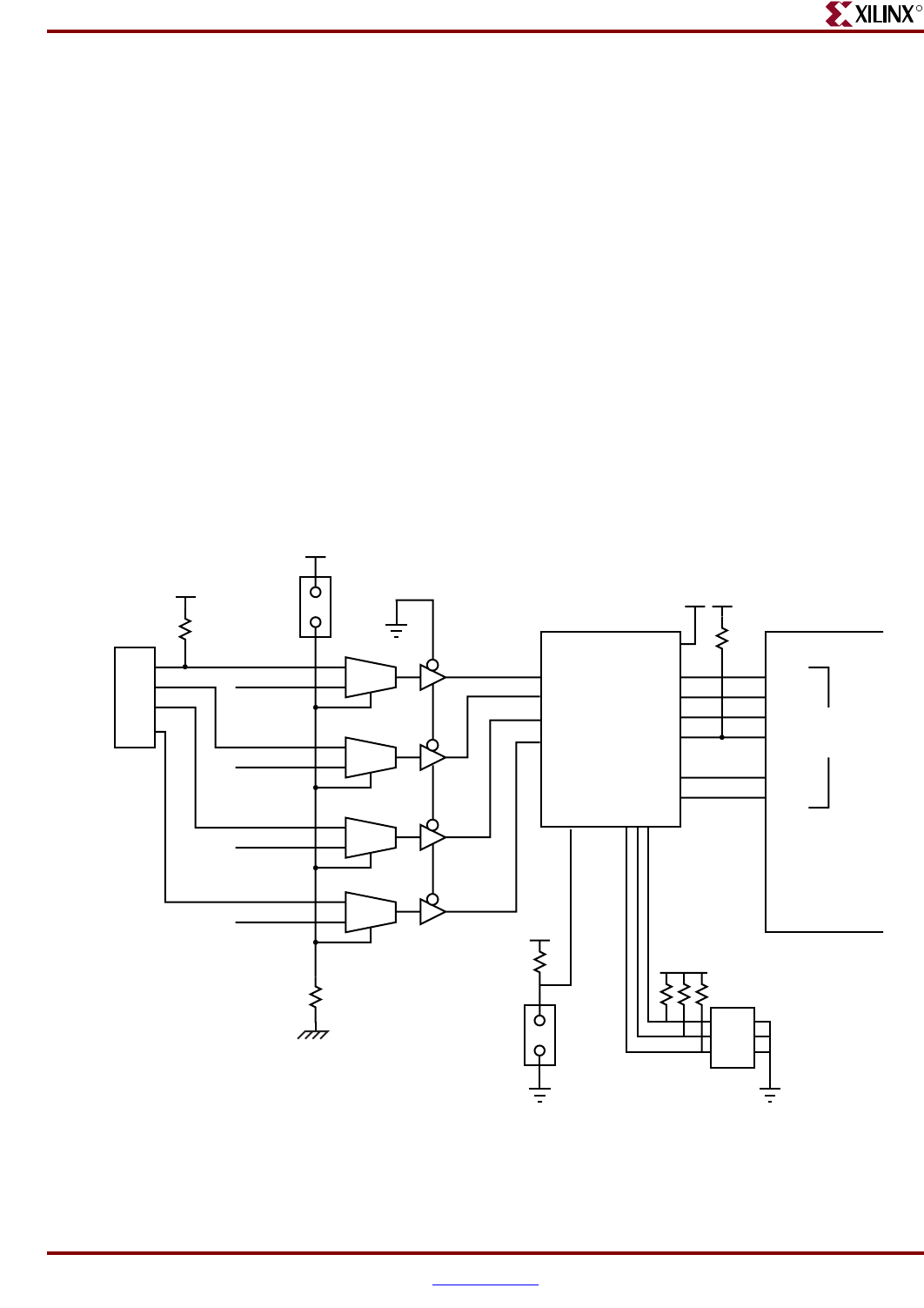
The JTAG connector initially connects to the System ACE chip, which passes the JTAG
connections through to the XC2VP30. Figure 2-6 is a block diagram showing the
connections between the JTAG connector, System ACE, and the XC2VP30. This diagram
also shows the logic that allows the CPU JTAG debug connector (J12) to be used to access
the JTAG interface to program the XC2VP30.
Figure 2-6: JTAG Connections to the XC2VP30 and System ACE
UG068_5_25_0805
0
J9 PC4
J19
U38
U37
System ACE XC2VP30
CPU_TCK
CPU_TMS
CPU_TDI
CPU_TDO
PC4_TCK
JTAG_SRC_SEL
TCK
TMS
TDI
TDO
TCK
TMS
TDI
TDO
PROG
2.5V
INIT
CFG_TCK
CFG_TMS
CFG_TDI
CFG_TDO
CFG_PROG
CFG_INIT
PC4_TMS
PC4_TDI
PC4_TDO
2.5V
0
1
3.3V
2.5V
0
1
0
1
0
1
J14
SW3
Schem Pg. 47
CF7
Mode
Pin
CFGADDR
Schem Pg. 20
2.5V
2.5V
2.5V


