ML310 User Guide www.xilinx.com 19
UG068 (v1.01) August 25, 2004 1-800-255-7778
Overview
R
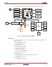
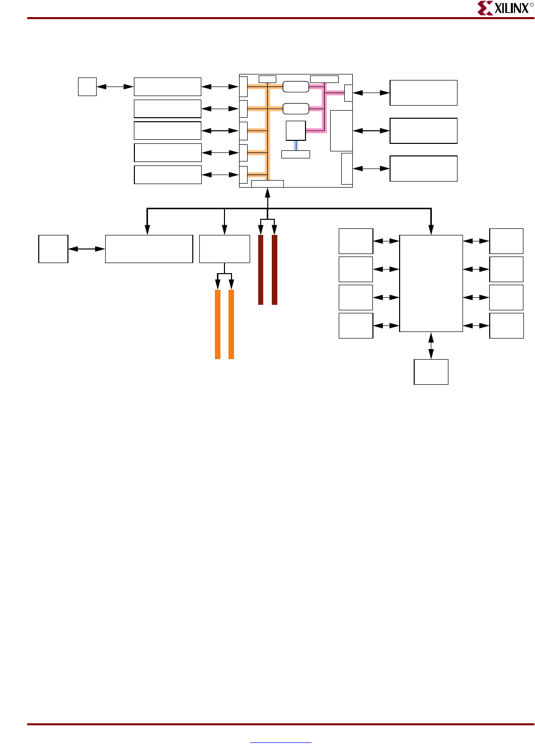
Figure 2-2 shows a high-level block diagram of the ML310 and its peripherals.
Features
In addition to the Virtex-II Pro™ FPGA with the embedded PPC405, the ML310 board
features the following:
• ATX Motherboard formfactor
• 256 MB DDR DIMM
• System ACE™ CF Controller
• 512 MB CompactFlash card
• Onboard 10/100 Ethernet NIC
• 4 PCI slots (3.3V and 5V)
• LCD character display and cable
• FPGA serial port connection
• RS-232 mini-cable
• Personality module interface for RocketIO and LVDS access
• Standard JTAG connectivity
• ALi Super I/O
♦ 1 parallel and 2 serial ports
Figure 2-2: ML310 High-Level Block Diagram
8 RocketIO MGTs
3 LVDS pairs
1 LVDS Clock pair
38 Single-Ended I/O
39 LVDS Pairs
1 Clock
256 MB
DDR DIMM
High-Speed
PM1
High-Speed
PM2
SMBus
RS232
System ACECF
SPI
GPIO / LEDs
PPC
405
PLB BRAM
PCI Bridge
OCM BRAM
DDR
UART SysACEGPIO SPI
INTC
PLB2OPB
Bridge
OPB2PLB
Bridge
PLB
Bus
OPB
Bus
OCM
Bus
SMBus
3.3V PCI
ALi
M1535D+
South Bridge
Intel GD82559
10/100 Ethernet NIC
RJ45
TI
PCI 2250
Audio
AMD
Flash
GPIO
IDE
(2)
USB
(2)
SMBus
Parallel
Port
PS/2
K/M
RS232
(2)
3.3V PCI
Slots
5V PCI
5V PCI
Slots
XC2VP30
FF896


