ML310 User Guide www.xilinx.com 65
UG068 (v1.01) August 25, 2004 1-800-255-7778
High-Speed I/O
R
PM1 Power and Ground
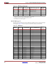
Table 2-29 shows the power and ground pins for the PM1 connector on the ML310.
PM2 Power and Ground
Table 2-30 shows the power and ground pins for the PM2 connector on the ML310.
ML310 PM User I/O Pins
PM1 User I/O
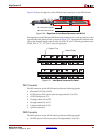
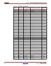
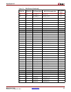
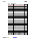
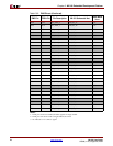
The PM1 connector makes the MGT signals from the eight RocketIO transceivers available
to the user, along with LVDS pairs and single-ended signals. Table 2-31 shows the pinout
for the PM1 connector on the ML310.
Table 2-29: PM1 Power and Ground Pins
Pin Number Description Length Contact Order
1, 6 Ground Level 4 First
2, 5 2.5V Level 3 Second
3 3.3V Level 2 Third
4 1.5V Level 2 Third
Table 2-30: PM2 Power and Ground Pins
Pin Number Description Length Contact Order
1, 6 Ground Level 4 First
2, 5 5V Level 3 Second
3, 4 12V Level 2 Third
Table 2-31: PM1 Pinout
PM1 Pin FPGA Pin Pin Description ML310 Schematic Net
FPGA Bank
V
CCO
A1 H26 IO_L32P_7 PM_IO_94 2.5V
A2 H25 IO_L32N_7 PM_IO_95 2.5V
A3 D26 IO_L03P_7 PM_IO_86 2.5V
A4 C26 IO_L03N_7 PM_IO_87 2.5V
A5 E13 IO_L46N_1 PM_IO_3V_25 3V
A6 E11 IO_L43P_1 PM_IO_3V_18 3V
A7 F10 IO_L07N_1 PM_IO_3V_7 3V
A8 H12 IO_L45P_1 PM_IO_3V_22 3V
A9 C7 IO_L08N_1 PM_IO_3V_9 3V
A10 D10 IO_L37N_1 PM_IO_3V_13 3V


