ML403 Board Information
XAPP979 (v1.0) February 26, 2007 www.xilinx.com 12
R
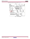
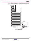
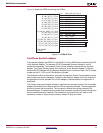
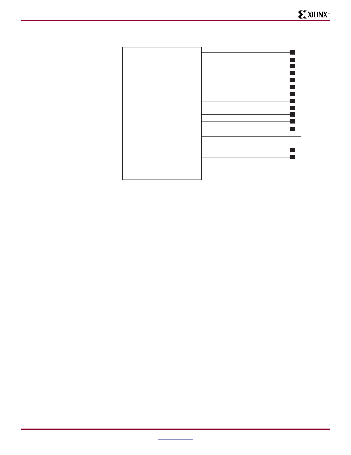
Figure 14 shows the FPGA pins driving the IIC Bus.
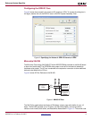
TotalPhase Aardvark Adapter
In the reference design, the OPB IIC in the XC4VFX12 on the ML403 board interfaces to the IIC
in the Aardvark Adapter. The Aardvark IIC/SPI Embedded Systems interface is a multi-
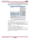
functional host adapter. The Aardvark Control Center software interacts with the Aardvark
Adapter. The Control Center controls the functionality of the Aardvark Adapter. It uses the
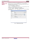
Aardvark IIC/SPI Software API. the Aardvark Adapter has six functional modes. The IIC-related
modes are the IIC + SPI and IIC Bus Monitoring modes.
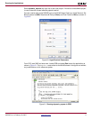
The Aardvark must be configured for use before the Aardvark Control Center software can be
used to send and receive messages. Configuring the Aardvark Adapter binds the instance of
the application with the available unit until the adapter is disconnected or the application is
terminated.
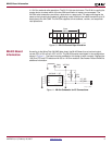
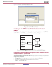
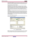
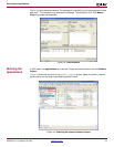
The Configure Aardvark Adapter window is organized into two major sections: list of available
adapters connected to the computer and list of the six operational modes. The main application
window is divided into two sections. The top section contains the modules used with the
Aardvark Adapter. The bottom section contains the transaction log which tracks all transactions
that the Aardvark sends or receives. The transaction log contains the time, read or write
transaction, master or slave, bit rate, address, number of bytes, and data.
Figure 14: FPGA IIC Pins
SMA_DIFF_CLK_IN_N
SMA_DIFF_CLK_IN_P
IIC_SCL
IIC_SDA
DDR_CLK1_N
DDR_CLK1_P
DDR_A13
DDR_BA1
DDR_BA0
DDR_CLK_P
MOUSE_DATA
PHY_TXCLK
C12
C13
A17
B17
B10
A10
A15
A16
B12
B13
C14
C15
GPIO_LED_2
GPIO_LED_3
MOUSE_CLK
PHY_RXC_RXCLK
A11
A12
B14
B15
IO_L8N_GC_LC_3_C12
IO_L8P_GC_LC_3_C13
IO_L7N_GC_LC_3_A17
IO_L6N_GC_LC_3_B10
IO_L7P_GC_LC_3_B17
IO_L6P_GC_LC_3_A10
IO_L5N_GC_LC_3_A15
IO_L5P_GC_LC_3_A16
IO_L4N_GC_VREF_LC_3_B12
IO_L4P_GC_LC_3_B13
IO_L3N_GC_LC_3_C14
IO_L3P_GC_LC_3_C15
IO_L2N_GC_VRP_LC_3_A11
IO_L2P_GC_VRN_LC_3_A12
IO_L1P_GC_CC_LC_3_B14
IO_L1P_GC_CC_LC_3_B15
FPGA_BANK3
2.5 VCC0
X979_14_012907


