


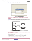
ML403 Board Information
XAPP979 (v1.0) February 26, 2007 www.xilinx.com 9
R
is ‘1010 for read and write operations. The A2, A1 bits are dont cares. The A0 bit is used by the
master device to select which of the two 256-word blocks of memory are accessed. The
24LC04 write transactions are either a byte write or a page write. The page write begins the
same as the byte write but instead of generating a stop condition the master transmits up to 16
data bytes to the 24LC04B. The 24LC04 supports current address, random, and sequential
read operations.
ML403 Board
Information
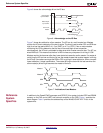
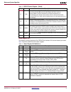
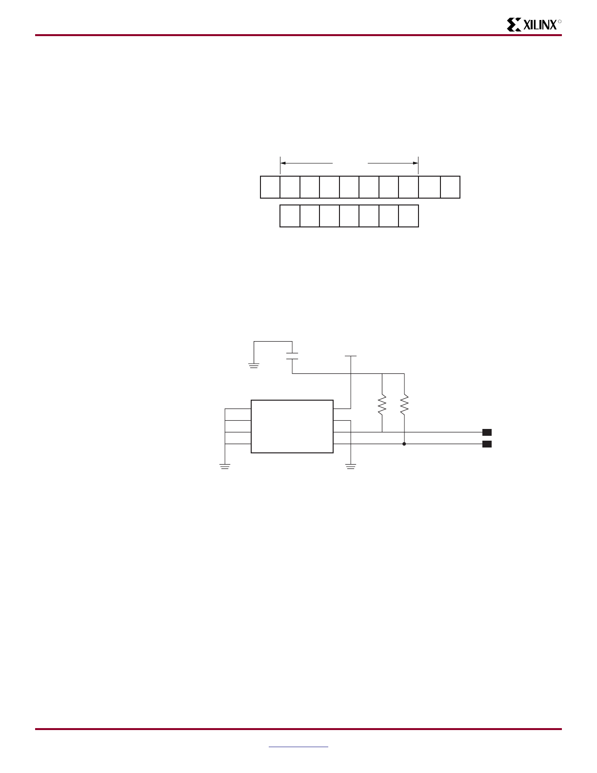
According to the MicroChip 24L024B data sheet, the ML403 board has a low-level output
current (IOL) of 3.0 mA at a VCC of 2.5v. The ML403 boards are shipped in the configuration
shown in Figure 11. The board must be modified for this design to work correctly. Replace the
10K Ohm R70 and R71resistors with 833 or 1K Ohm resistors. See Answer Record 24049 for
additional information.
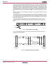
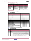
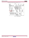
Figure 10: 24LC04 Control Byte Allocation
Slave
Address
AR/W
S
A01
X979_10_012907
010A2A1
Figure 11: ML40x Schematic for IIC Connections
24LC04B - I / ST
VCC2V5
IIC_SCL
IIC_SDA
A0
A1
A2
A3
VCC
WP
SCL
SDA
TSSOPSU9
1
2
3
4
8
7
6
5
R71
10k
R70
10k
C280
0.1 µF
1
2
1
2
X979_11_022307