


Introduction
XAPP979 (v1.0) February 26, 2007 www.xilinx.com 3
R
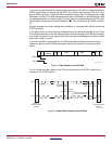
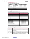
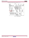
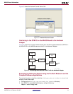
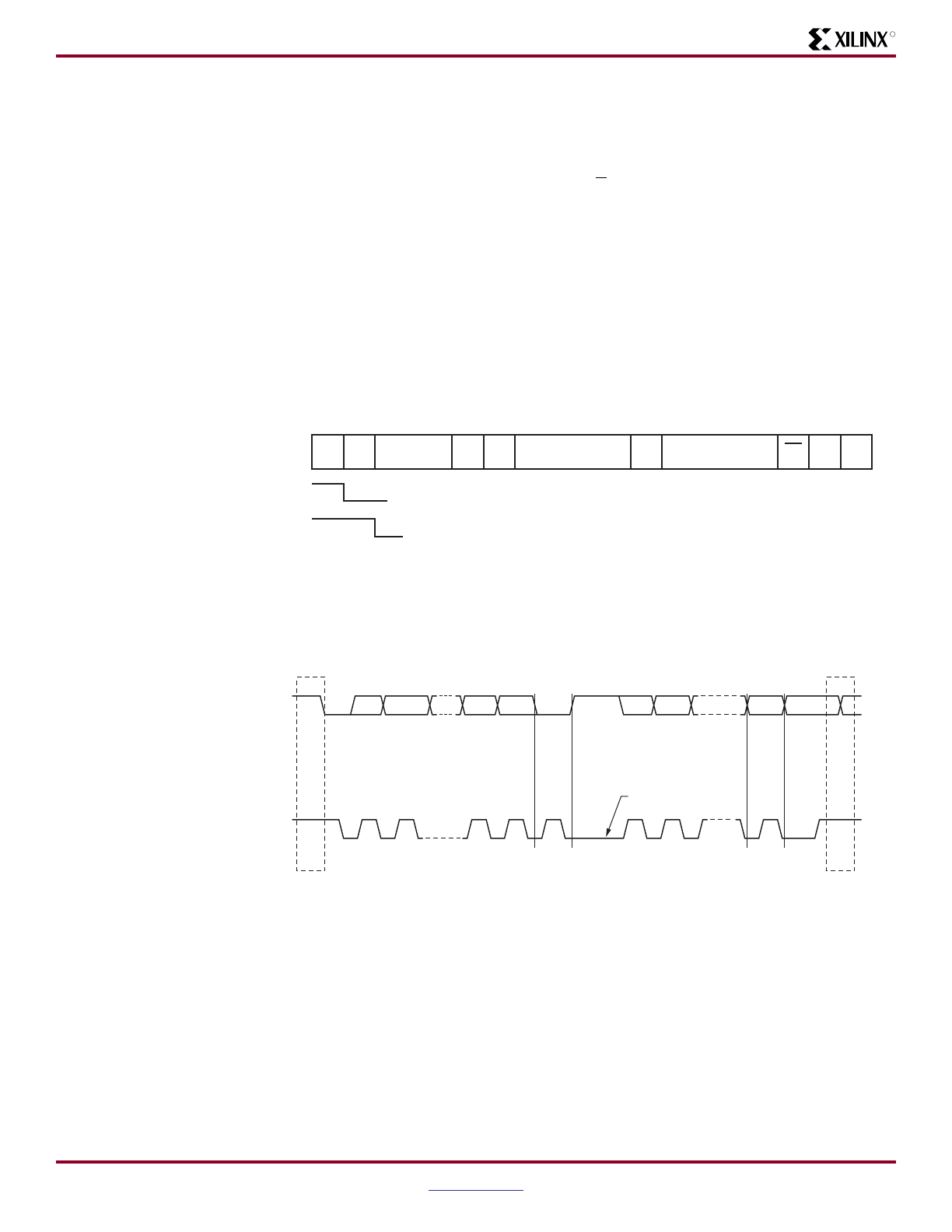
Figure 4 shows the format of the data transfer of two bytes on the IIC bus, beginning with the
START (S) condition and ending with the STOP (P) condition, bounded by an idle IIC (F) bus.
After a START condition, an eight bit field is transmitted containing a 7 bit address and a single
Read/Write (R/W) bit. This 8 bit address/direction field is followed by an Acknowledge bit. After
the address/data field, an eight bit data field is followed by an acknowledge bit (A). The last 8-
bit data field is followed by a not acknowledge bit (A). This is followed by the STOP condition
(P).
A single message can contain multiple start conditions, or a repeated start, without intervening
STOP conditions.
In this data transfer, there are two acknowledge bits and one Not Acknowledge on the IIC bus.
The distinction between a Not Acknowledge and a No Acknowledge is that Not Acknowledge
occurs after a master has read a byte from a slave and a No Acknowledge occurs after a master
has written a byte to a slave.
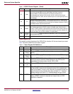
A synchronized SCL is generated with its LOW period determined by the device with the
longest low period and its HIGH period determined by the device with the shortest HIGH
period.
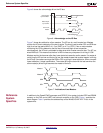
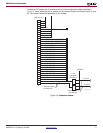
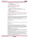
Figure 5 shows the data transfer on the IIC bus, beginning with the START condition and
ending with the STOP condition.
Figure 4: Data Transfer on the IIC Bus
Figure 5: Generic Data Transer on the IIC Bus
SDA
Slave
Address
FAAR/WS PF
SCL
X979_04_012907
Data Data
A
12 127 8 9 3 - 8 9
Acknowledgment
signal from slave
Acknowledgment
signal from receiver
Byte complete;
interrupt within slave
Clock lines held low while
interrupts are serviced
S
or
SR
Sr
or
P
P
Sr
X979_05_022307
START or
repeated START
condition
STOP or
repeated START
condition
MSB
SCL
SDA
ACKACK