


Introduction
XAPP979 (v1.0) February 26, 2007 www.xilinx.com 2
R
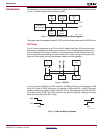
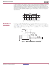
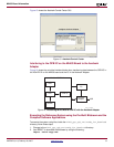
Introduction This application note accompanies a reference system built on the ML403 development board.
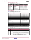
Figure 1 is a block diagram of the reference system.
The system uses the embedded PowerPC (PPC) as the microprocessor and the OPB IIC core.
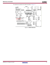
IIC Primer
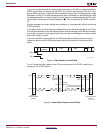
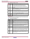
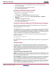
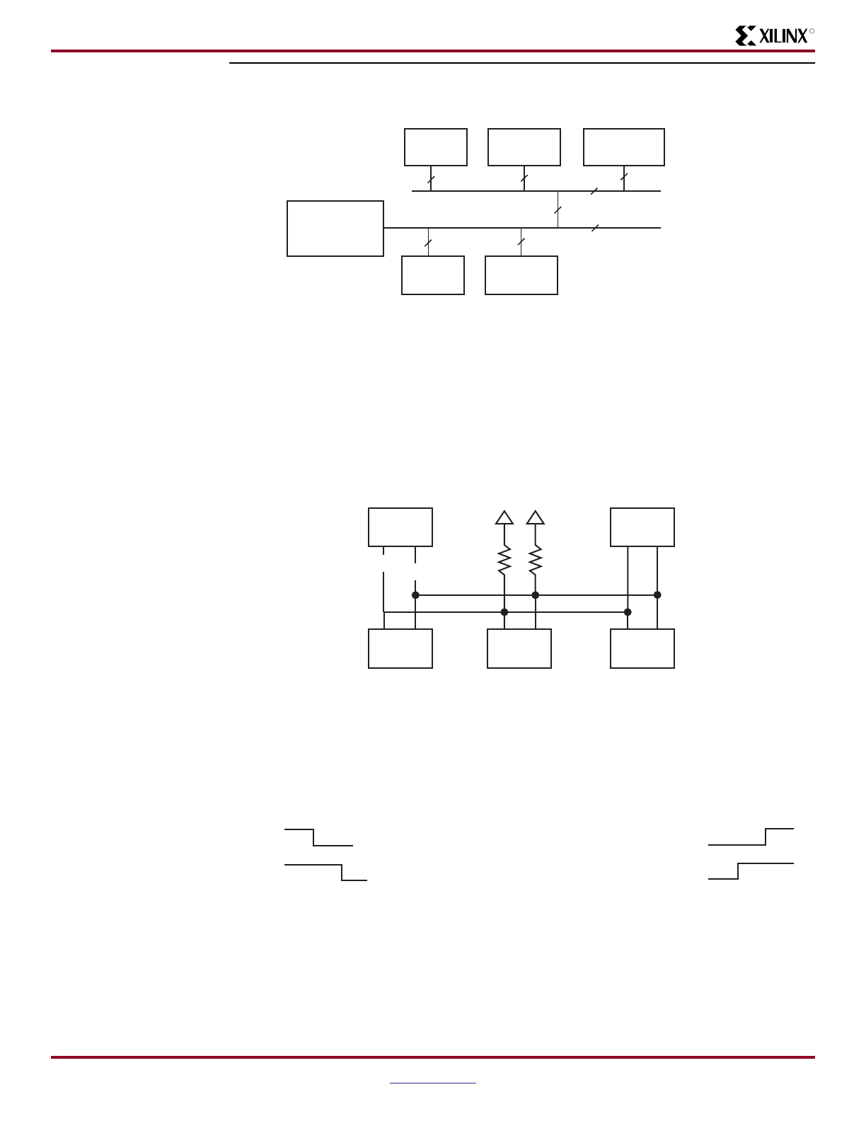
Figure 2 shows components on an IIC bus.Two IIC masters and three IIC slaves are shown.
The master is responsible for setting up transactions. This includes generating the clock on
SCL and defining which slave is involved in the communication, with an address field, and
which component is transmitting and which component is receiving. Some components are
slave only, while others can transition between master and slave operation.
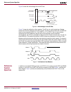
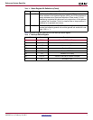
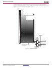
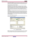
Figure 3 shows the START and STOP conditions. A START condition is a falling edge on SDA
when SCL is high. A STOP condition is a rising edge on SDA when SCL is high. During data
transfer, the data line is stable on SDA when SCL is high. Data transitions on SDA when SCL
is low. Note that the START and STOP conditions are special conditions, violating the rule that
data cannot transition while SCL is high.
Figure 1: OPB IIC Reference System Block Diagram
Figure 2: IIC Bus
Figure 3: Start and Stop Conditions
PowerPC™
405 Processor
OPB
INTC
OPB UART
16550
PLB
DDR
PLB
BRAM
OPB
IIC
OPB
PLB
X979_01_022307
S1 S2
M1 M2
S3
X979_02_022307
SCL
SDA
X979_03_022307
SDA
Start Stop
SCL