


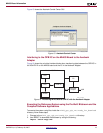
Reference System Specifics
XAPP979 (v1.0) February 26, 2007 www.xilinx.com 5
R
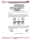
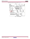
ML403 XC4VFX12 Address Map
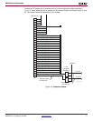
OPB IIC Registers
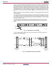
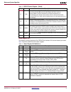
Table 2 provides the register map for the OPB IIC core.
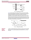
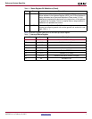
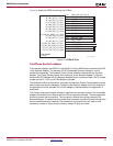
Table 3 provides a description of the OPB IIC control register.
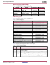
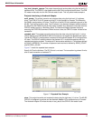
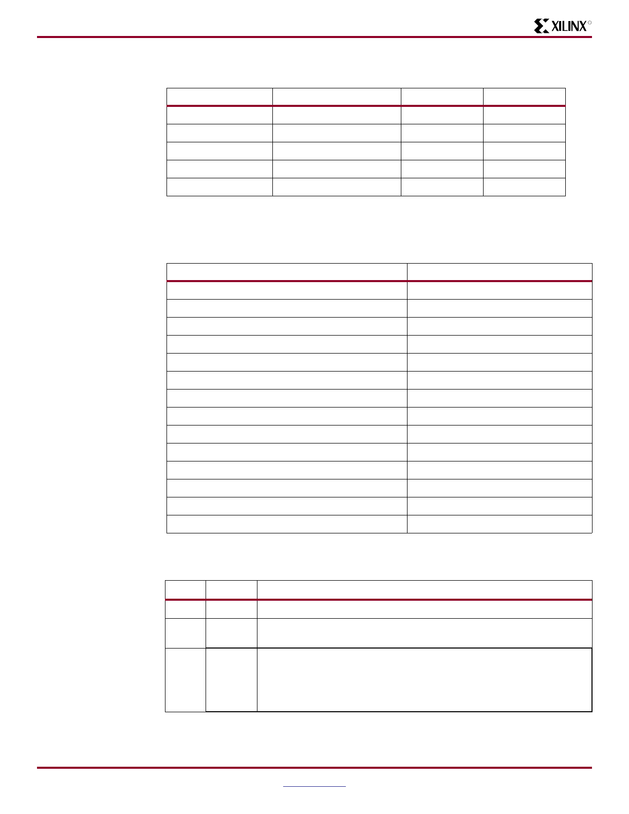
Table 1: ML403 XC4VSX12 System Address Map
Peripheral Instance Base Address High Address
PLB_DDR DDR_SDRAM_32Mx64 0x00000000 0x03FFFFFF
OPB UART16550 RS232_Uart_1 0x40400000 0x4040FFFF
OPB INTC opb_intc_0 0x41200000 0x4120FFFF
PLB BRAM plb_bram_if_cntlr_0 0xFFFF8000 0xFFFFFFFF
OPB IIC IIC_EEPROM 0x40800000 0x4080FFFF
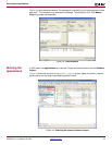
Table 2: OPB IIC Registers
Register Address
Device Global Interrupt Enable C_BASEADDR + 0x01C
Interrupt Status Register C_BASEADDR + 0x020
Interrupt Enable Register C_BASEADDR + 0x028
Software Reset Register C_BASEADDR + 0x040
Control Register C_BASEADDR + 0x100
Status Register C_BASEADDR + 0x104
Transmit FIFO C_BASEADDR + 0x108
Receive FIFO C_BASEADDR + 0x10C
Slave Address Register C_BASEADDR + 0x110
Transmit FIFO Occupancy C_BASEADDR + 0x114
Receive FIFO Occupancy C_BASEADDR + 0x118
Ten Bit Slave Address Register C_BASEADDR + 0x11C
Receive FIFO Programmable Depth Interrupt Register C_BASEADDR + 0x120
General Purpose Output C_BASEADDR + 0x124
Table 3: OPB IIC Control Register
Bit(s) Name Description
0- 24 Reserved Reserved.
25 GC_EN
General Call Enable. Setting this bit High allows the OPB IIC to respond to a
general call address.
26 RSTA
Repeated Start. Writing a “1” to this bit generates a repeated START condition
on the bus if the OPB IIC Bus Interface is the current bus Master. Attempting a
repeated START at the wrong time, if the bus is owned by another Master, results
in a loss of arbitration. This bit is reset when the repeated start occurs. This bit
must be set prior to writing the new address to the Tx FIFO or DTR.