CY7C601xx, CY7C602xx
Document 38-16016 Rev. *E Page 17 of 68
11.5.3 WriteBlock Function
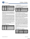
The WriteBlock function is used to store data in Flash. Data is
moved 64 bytes at a time from SRAM to Flash using this function.
The WriteBlock function first checks the protection bits and deter-
mines if the desired BLOCKID is writable. If write protection is
turned on, the WriteBlock function exits setting the accumulator
and KEY2 back to 00h. KEY1 has a value of 01h, indicating a
write failure. The configuration of the WriteBlock function is
straightforward. The BLOCKID of the Flash block, where the
data is stored, is determined and stored at SRAM address FAh.
The SRAM address of the first of the 64 bytes to be stored in
Flash is indicated using the POINTER variable in the parameter
block (SRAM address FBh). Finally, the CLOCK and DELAY
value are set correctly. The CLOCK value determines the length
of the write pulse used to store the data in Flash. The CLOCK
and DELAY values are dependent on the CPU speed and must
be set correctly. Refer to the Clocking section for additional infor-
mation.
11.5.4 EraseBlock Function
The EraseBlock function is used to erase a block of 64
contiguous bytes in Flash. The EraseBlock function first checks
the protection bits and determines if the desired BLOCKID is
writable. If write protection is turned on, the EraseBlock function
exits setting the accumulator and KEY2 back to 00h. KEY1 has
a value of 01h, indicating a write failure. The EraseBlock function
is only useful as the first step in programming. Erasing a block
does not make data in a block fully unreadable. If the objective
is to obliterate data in a block, the best method is to perform an
EraseBlock followed by a WriteBlock of all zeros.
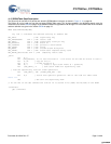
To set up the parameter block for EraseBlock, correct key values
must be stored in KEY1 and KEY2. The block number to be
erased is stored in the BLOCKID variable and the CLOCK and
DELAY values are set based on the current CPU speed.
11.5.5 ProtectBlock Function
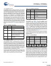
The enCoRe II LV devices offer Flash protection on a
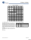
block-by-block basis. Table 11-7 lists the protection modes
available. In the table, ER and EW indicate the ability to perform
external reads and writes; IW is used for internal writes. Internal
reading is always permitted using the ROMX instruction. The
ability to read using the SROM ReadBlock function is indicated
by SR. The protection level is stored in two bits according to
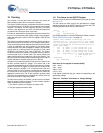
Table 11-7. These bits are bit packed into 64 bytes of the
protection block. Therefore, each protection block byte stores
the protection level for four Flash blocks. The bits are packed into
a byte, with the lowest numbered block’s protection level stored
in the lowest numbered bits in Table 11-7.
The first address of the protection block contains the protection
level for blocks 0 through 3; the second address is for blocks 4
through 7. The 64th byte stores the protection level for blocks
252 through 255.
Only an EraseAll decreases the protection level by placing zeros
in all locations of the protection block. To set the level of
protection, the ProtectBlock function is used. This function takes
data from SRAM, starting at address 80h, and ORs it with the
current values in the protection block. The result of the OR
operation is then stored in the protection block. The EraseBlock
function does not change the protection level for a block.
Because the SRAM location for the protection data is fixed and
there is only one protection block per Flash macro, the Protect-
Block function expects very few variables in the parameter block
to be set before calling the function. The parameter block values
that are, besides the keys, are the CLOCK and DELAY values.
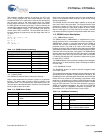
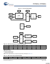
Table 11-5. WriteBlock Parameters
Name Address Description
KEY1 0,F8h 3Ah
KEY2 0,F9h Stack Pointer value, when SSC is
executing
BLOCK ID 0,FAh 8 KB Flash block number (00h–7Fh)
4 KB Flash block number (00h–3Fh)
3 KB Flash block number (00h–2Fh)
POINTER 0,FBh First 64 addresses in SRAM where
the data is stored in Flash is located
before calling WriteBlock
CLOCK 0,FCh Clock Divider used to set the write
pulse width
DELAY 0,FEh For a CPU speed of 12 MHz set to 56h
Table 11-6. EraseBlock Parameters
Name Address Description
KEY1 0,F8h 3Ah
KEY2 0,F9h Stack Pointer value, when SSC is
executed
BLOCKID 0,FAh Flash block number (00h–7Fh)
CLOCK 0,FCh Clock Divider used to set the erase
pulse width
DELAY 0,FEh For a CPU speed of 12 MHz set to
56h
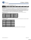
Table 11-7. Protection Modes
Mode Settings Description Marketing
00b SR ER EW IW Unprotected Unprotected
01b SR
ER EW IW Read protect Factory upgrade
10b SR
ER EW IW Disable external
write
Field upgrade
11b SR
ER EW IW Disable internal
write
Full protection
76543210
Block n+3 Block n+2 Block n+1 Block n
[+] Feedback [+] Feedback


