


CY7C601xx, CY7C602xx
Document 38-16016 Rev. *E Page 5 of 68
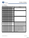
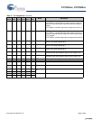
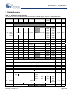
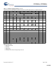
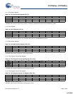
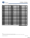
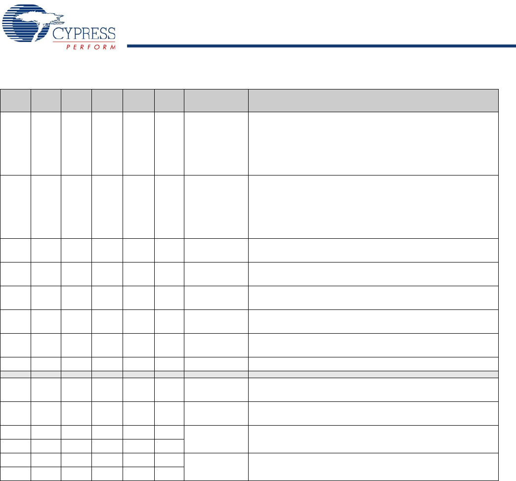
23 19 13 9 9 16 P0.0/CLKIN GPIO Port 0 bit 0—Configured individually
On CY7C601xx, optional Clock In when external oscillator is
disabled or external oscillator input when external oscillator is
enabled.
On CY7C602xx, oscillator input when configured as Clock In.
22 18 12 8 8 15 P0.1/CLKOUT GPIO Port 0 bit 1—Configured individually
On CY7C601xx, optional Clock Out when external oscillator is
disabled or external oscillator output drive when external oscil-
lator is enabled.
On CY7C602xx, oscillator output when configured as Clock Out.
21 17 11 7 7 14 P0.2/INT0 GPIO port 0 bit 2—Configured individually
Optional rising edge interrupt INT0.
20 16 10 6 6 13 P0.3/INT1 GPIO port 0 bit 3—Configured individually
Optional rising edge interrupt INT1.
19 15 9 5 5 12 P0.4/INT2 GPIO port 0 bit 4—Configured individually
Optional rising edge interrupt INT2.
18 14 8 4 4 11 P0.5/TIO0 GPIO port 0 bit 5—Configured individually
Alternate function timer capture inputs or timer output TIO0.
17 13 7 3 3 10 P0.6/TIO1 GPIO port 0 bit 6—Configured individually
Alternate function timer capture inputs or timer output TIO1.
16 12 6 2 2 9 P0.7 GPIO port 0 bit 7—Configured individually
1,2,3,
4
1 1 7 NC No connect
45,46,
47,48
12 24 8 NC No connect
5117 V
DD
Power
27 23 1 16 15 22
44 40 14 – – – V
SS
Ground
24 20 28 13 12 19
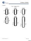
Table 6-1. Pin Assignments (continued)
48
SSOP
40
PDIP
28
SSOP
24
QSOP
24
SOIC
24
PDIP
Name Description
[+] Feedback [+] Feedback