


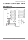
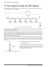
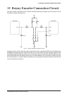
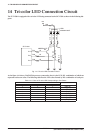
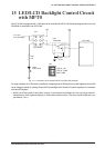

10 POWER CONTROL CIRCUIT FOR BATTERY BACKUP FUNCTION
30
EPSON
S5U1C17801T1100 HARDWARE MANUAL
(SOFTWARE EVALUATION TOOL FOR S1C17801)
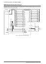
#STBY Pin
This pin is used to disconnect the RTCVDD line from the VDD line (AVDD line) electrically.
If a LOW signal is input to the pin, area covered by the RTCV
DD line becomes electrically independent of other
area. Stopping power supply to the V
DD line (AVDD line) while a high signal is input causes inconstant signals
to be entered into RTC or IVRAM, or current to be leaked from the RTCV
DD line to the VDD line. Therefore, be
sure to input a LOW signal to #STBY pin before stopping power supply to the V
DD line (AVDD line).
∗ Notes: The RTCVDD area cannot be accessed while the #STBY pin is in LOW status. A HIGH signal must be
output from P43 to make the #STBY pin HIGH status before gaining access to the RTCV
DD area.
WAKEUP Pin
This signal pin is used to restore the SVT17801 from battery backup status to normal status.
The V
DD and AVDD lines can be turned on using the WAKEUP pin. For the SVT17801, this pin is connected to
the ENABLE pin on regulator,and so the power supply can be resumed by outputting a HIGH signal to the EN-
ABLE pin.
The WAKEUP pin can be controlled by using RTC.
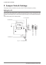
JP2 and JP3 Settings
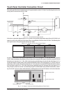
In order to enable backup battery function on the circuit installed on SVT17801 as shown in the figure 10.2.1,
JP2 and JP3 must be set to WAKEUP ENABLE and Battery respectively (both factory default).
JP2 is located just before the WAKEUP pin s entering into an OR circuit, and if JP2 is set to WAKEUP DIS-
ABLE, 5V instead of WAKEUP pin is input to the OR circuit, turning regulator always ON.
JP3 selects supply source of RTCV
DD shown in the figure 10.2.1. If Battery is selected, RTCVDD is supplied
from the coin cell battery (CR2032) and if V
DD is selected, RTCVDD is supplied from VDD. For detail of JP set-
tings, see Chapter 8.
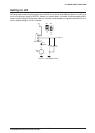
RSTO (Power Switch) and WAKEUP Pin
The following list shows GPIO (PC2) status and VDD voltage according to power switch and WAKEUP pin
statuses when JP1 and JP2 are set to EnableWakeup and Battery respectively in the circuit shown in the figure
10.2.1.
Table 10.2.1 PC2 and VDD Status According to Power Switch and WAKEUP Pin
Power Switch WAKEUP (HIGH Active) GPIO(PC2) VDD (V)
CLOSE (being pressed) HIGH HIGH 3.3
OPEN HIGH LOW 3.3
CLOSE (being pressed) LOW HIGH 3.3
OPEN LOW LOW 0
GPIO(PC2) is a signal representing OPEN/CLOSE status of power switch, and used when controlling power
supply.
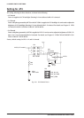
Shifting to Standby Mode
The following is an example to show how to set up standby mode in the circuit shown in the figure 10.2.1.
➀ Set JP1 to EnableWakeup and turn the system power (VDD) on.
➁ CPU starts working.
➂ After setting P43 to HIGH output and the STBY pin to HIGH, set WAKEUP to HIGH active and
WAKEUP output signal to HIGH. (to enable WAKEUP status)
• • •
➃ Press power switch. (Pressing the power switch turns PC2 HIGH.)
➄ If PC2s HIGH status is detected, set P43 to HIGH output and the STBY pin to HIGH (to enable write
to IVRAM inside RTC).
➅ Write RTC setting data to IVRAM.