


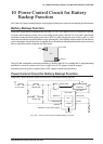

10 POWER CONTROL CIRCUIT FOR BATTERY BACKUP FUNCTION
S5U1C17801T1100 HARDWARE MANUAL
EPSON
31
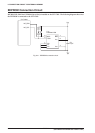
(SOFTWARE EVALUATION TOOL FOR S1C17801)
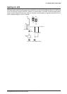
➆ Set the WAKEUP signal to LOW. → ∗ The power switch is being pressed during above steps.
➇ Setting for standby mode has been completed. (RTCVDD is running in ON status.)
After
➇, the VDD line (AVDD line) can be turned off.
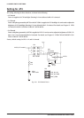
Releasing Standby Mode
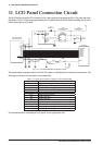
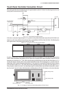
The following is an example to show how to release standby mode in the circuit shown in the figure 10.2.1.
(Example 1)
➀ In Step ➄ of above set-up example 1, the standby mode is released (WAKEUP pin is turned HIGH) af-
ter predefined time has passed, and the output of regulator shown in figure 10.2.1 becomes always 3.3V.
(Example 2)
➀ Press power switch.
➁ While the power switch is being pressed, the output of regulator shown in figure 10.2.1 becomes 3.3V,
S1C17801 starts operating and, immediately after that, the standby mode is released by turning the
WAKEUP signal HIGH.
➂ By turning the WAKEUP signal HIGH at Step ➁, the output of regulator shown in figure 10.2.1 be-
comes always 3.3V.
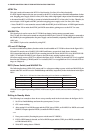
∗ This power control circuit should be used only for reference. The circuit is designed for reducing the current con-
sumption of whole system by turning the V
DD line (AVDD line) off. This technique is effective for the case where
the V
DD line (AVDD line) has a longer power-off time, or a board has many peripheral parts with relatively HIGH
current consumption. Other technique (such as Sleep or Halt) may still be advantageous depending on your ap-
proach to control the overall system. We recommend you review all necessary factors to choose the optimal way
when you design a total system.