


20 EXCLUSIVE CONTROL OF PORTS
S5U1C17801T1100 HARDWARE MANUAL
EPSON
43
(SOFTWARE EVALUATION TOOL FOR S1C17801)
20 Exclusive Control of Ports
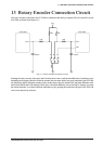
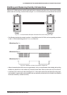
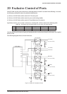
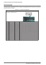
The SVT17801 uses five ports exclusively by connecting them to switch ICs as shown in the following. As a result,
the following combination cannot be operated simultaneously.
(1) Write to NAND Flash and the control of LCD touch panel.
(2) Write to NAND Flash and the control of power switch using standby.
(3) Write to NAND Flash and the control of 7th pin/9th pin on J8 connector.
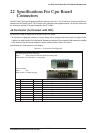
Specifically, the five ports are used exclusively by switching H/L of P45 as shown in the following table.
Table 20.1 P45 Status and Connection Status of PC3, PC2, P34, P33, and PA2
P45 PC3 PC2 P34 P33 PA2
H NAND Flash NAND Flash NAND Flash NAND Flash NAND Flash
L J8 connector
Power switch
LCD module LCD module J8 connector
Note that the P45 port becomes an input port immediately after reset has been released. In this status, P45 is pulled
down to LOW.
The following diagram shows a circuit in this area.
VDD
C50 0.1µF
R67
10K
R84
47K
4
6
1
3
4
6
1
3
4
6
1
3
4
6
1
3
4
6
V G
V G
V G
V G
V G
1
3
R71
10K
R68
10K
R56
10K
5
2
VDD
C40 0.1µF
5
2
VDD
C39 0.1µF
5
2
V
DD
C28 0.1µF
5
2
VDD
C27 0.1µF
U27 TS5A3159A
ALE (NAND)
7pin (J8 connector)
CLE (NAND)
POWER SW
WE (NAND)
TOP
(LCD module)
S1C17801
PC3
PC2
P34
P45
P33
PA
2
U28 TS5A3159A
U29 TS5A3159A
U30 TS5A3159A
U31 TS5A3159A
5
2
RE (NAND)
LEFT (LCD module)
CE (NAND)
9pin (J8 connector)
Fig. 20.1 Switch IC Connection Circuit