


EPSON FX-2180 Service Manual Chapter 2 Operating Principles
2-3
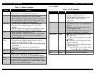
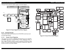
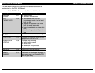
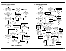
The figure below shows the power supply circuit block diagram.
filter circuit
full-wave
rectification
circuit
smoothing
circuit
switching
circuit
AC input
smoothing
circuit
+5 V switching
regulator
+5 V over-current
protection circuit
+35 VDC
+5 VDC
photo-
coupler
photo-
coupler
+35 V line
over-voltage
protection circuit
+35 V line
overload
detector circuit
+35 V line
over-current
protection circuit
Operate
(power) button
secondary circuit
CPU
port 20
+35 V line
constant voltage
control circuit
+5 V line
over-voltage
protection circuit
+5 V constant voltage
control circuit
voltage
doubler
rectification
automatic
switching
circuit
C244 PSH only
primary circuit
Figure 2-2. Power Supply Circuit Block Diagram
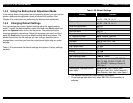
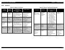
2.1.3 Control Circuit
The printer’s control circuit consists of the C244 MAIN control board and
the control panel board.
2.1.3.1 Control Circuit Operation
The control circuit includes a TMP96C141BF CPU that runs at 17.20 MHz,
an E05B50** gate array, a 2 Mbit PROM (or 2 Mbit / 4 Mbit flash ROM), a 1
Mbit / 4 Mbit PS-RAM (or SRAM), a serial (or parallel) EEPROM, and other
circuits. The control circuit controls all the printer’s components. Figure 2-3
shows the control circuit block diagram.
gate array
CPU
CSF driver
CSF
sensor
rear PE
sensor
front PE
sensor
TOP
sensor
home
position
sensor
paper
release
lever sensor
platen gap
lever
sensor
+35 V voltage
sensor
print head
driver
print head
temperature
sensor
EPROM
PS-RAM
or SRAM
serial
EEPROM
reset IC
PF driver CR driver
control panel
buttons & LEDs
Operate button
parallel I/F
type B I/F
5 V
GL
35 V
GP
IC2
IC1
E05B50**
TMP96C141BF
Q2-Q19
IC12
SLA7024M
UDN2917EB
IC8
IC15
: data bus
: address bus
IC3
IC5
PSC
PWDN
power supply
board
IC9
Figure 2-3. Control Circuit Block Diagram