20 Design Guide
Intel
®
31244 PCI-X to Serial ATA Controller
Intel
®
31244 PCI-X to Serial ATA Controller Package
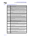
P_REQ64#
BIDIRECTIONAL - LVTTL: Indicates the attempt of a 64-bit transaction on the PCI bus.
When the target is 64-bit capable, the target acknowledges the attempt with the assertion of
P_ACK64#.
P_RST#
INPUT - LVTTL Reset: This signal is used to place PCI-X registers, sequencers, and
signals into a consistent state. When P_RST# is asserted, all PCI-X output signals are
tri-stated.
P_SERR#
OUTPUT - Open Drain with Pull-Up Resistor: System Error. This signal is used to report
address parity errors. When an error is detected, P_SERR# is driven LOW for a single
PCI-X clock.
P_STOP#
BIDIRECTIONAL - LVTTL with Pull-Up Resistor: Stop. This signal is driven by the target
to indicate to the initiator that it wishes to stop the current transaction. As a bus slave,
P_STOP# is driven by the GD31244 to inform the bus master to stop the current transaction.
As a bus master, P_STOP# is received by the GD31244 to stop the current transaction.
P_TRDY#
BIDIRECTIONAL - LVTTL with Pull-Up Resistor: Target Ready. This signal indicates the
selected device’s ability to complete the current data phase and is used in conjunction with
P_IRDY#. A data phase is completed on any clock cycle where both P_IRDY# and
P_TRDY# are asserted LOW.
TEST0 INPUT - LVTTL: Test input. Set LOW for normal operation.
TOUT OUTPUT - Test pin. Do not use.
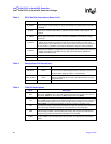
Table 5. Configuration Pin Descriptions
Name Type Description
32BITPCI# INPUT
Pin number A2. This pin controls the state of the “64 bit device” status
bit 16, in the PCI-X Status Register. When pulled down, reports a 0, a
32-bit bus. When pulled up, reports 1, a 64-bit device.
DPA_MODE# INPUT
INPUT - LVTTL: When HIGH or open, selects Master/Slave Mode for
software compatibility. When LOW, selects Master-Master mode for
high performance.
SSCEN INPUT Tie this pin to GND.
Table 6. JTAG Pin Descriptions
Name Description
TDO
TEST DATA OUTPUT: is the serial output pin for the JTAG feature. TDO is driven on the
falling edge of TCK during the SHIFT-IR and SHIFT-DR states of the Test Access Port. At
other times, TDO floats. The behavior of TDO is independent of P_RST#.
TDI
TEST DATA INPUT: is the serial input pin for the JTAG feature. TDI is sampled on the rising
edge of TCK, during the SHIFT-IR and SHIFT-DR states of the Test Access Port. This signal
has a weak internal pull-up to ensure proper operation when this signal is unconnected.
TCK
TEST CLOCK: is an input which provides the clocking function for the IEEE 1149.1
Boundary Scan Testing (JTAG). State information and data are clocked into the component
on the rising edge and data is clocked out of the component on the falling edge.
TMS
TEST MODE SELECT: is an input sampled at the rising edge of TCK to select the operation
of the test logic for IEEE 1149.1 Boundary Scan testing. This signal has a weak internal
pull-up to ensure proper operation when this signal is unconnected.
TRST#
TEST RESET: an input that asynchronously resets the Test Access Port (TAP) controller
function of IEEE 1149.1 Boundary Scan Testing (JTAG). This signal has a weak internal
pull-up.
Table 4. PCI-X Bus Pin Descriptions (Sheet 2 of 2)
Name Description


