Design Guide 21
Intel
®
31244 PCI-X to Serial ATA Controller
Intel
®
31244 PCI-X to Serial ATA Controller Package
3.1.1 VA0, VA1 (V
CCPLL
) Pin Requirements
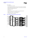
To reduce clock skew, the VA0 and VA1 balls for the Phase Lock Loop (PLL) circuit are each
isolated on the package. The lowpass filter, as shown in Figure 2, reduces noise induced clock jitter
and its effects on timing relationships in system designs. The 22 µF bulk capacitors must be low
ESR solid tantalum and the 0.1 µF ceramic capacitor must be of the type X7R. The node
connecting VA0 and VA1, must be as short as possible.
Table 7. Serial ROM Interface Pin Descriptions
Name Description
SDI
INPUT - LVTTL with Pull Up: Connects to the serial data output (SDO) of the Serial ROM.
Customers are recommended to add pads for both a pull-up and a pull-down resistor for
possible use in the future.
SDO (LED3)
OUTPUT - LVTTL: Connects to the serial data input (SDI) of the Serial ROM. This is also
the activity LED output for Channel 3 when all four LEDs are activated (active LOW).
SCLK (LED2)
OUTPUT - LVTTL: Connects to the clock input (SCLK) of the serial ROM. This is also the
activity LED output for Channel 2 when all four LEDs are activated (active LOW).
SCS#
OUTPUT - LVTTL with Pull Up: Connects to the chip select input (SCS#) of the Serial
ROM.
Table 8. Power Supply Pin Descriptions
Name Description
V18A, V18B
OUTPUT: This is the regulated 1.8 V supply generated internally. Bypass with 0.1 and 10 µF
capacitors.
V18A and V18B are each outputs of internal voltage regulators. They need to be separately
bypassed to ground with 0.1 and 10 µF capacitors separately, they must not be connected
together.
V
CC5REF
Voltage Clamp I/O: In 5 V tolerant systems, this is connected to a 5 V supply. In 3.3 V
powered systems this is connected to 3.3 V. In PCI add-in cards, this is normally connected
to I/O Power (10 A, 16 A, 19 B, 59 A and 59 B). The user must ensure that the value of
V
CC5REF
is high enough to ensure compliance to the V
IH(MAX)
specification on every input to
the GD31244 not just PCI inputs. For example, when the Serial ROM device is 5 V I/O this
pin must be 5 V regardless of the PCI bus.
VA0, VA1
2.5 V Analog Power Supply: Separate filtering is recommended. VA0 supplies the PCI
PLL. VA1 supplies the CMU.
V
SS
Ground.
V
CC
2.5 V Digital Logic Power Supply.
V
IO
3.3 V PCI I/O Power Supply.
V
CC0
, V
CC1
,
V
CC2
, V
CC3
2.5 V High-Speed I/O Power Supply for each channel.


