44 Design Guide
Intel
®
31244 PCI-X to Serial ATA Controller
Printed Circuit Board (PCB) Methodology
6.2.3 Backplane Stripline Stackup
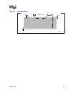
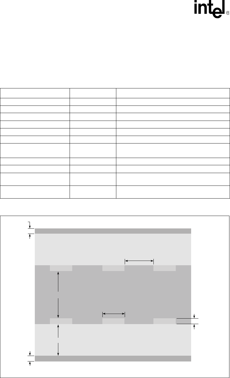
Figure 16 provides an example stackup that may be used to implement the backplane design. The
stripline shown in Figure 16 is implemented with ground flood on both component and solder side
of the PCB. The differential stripline traces are etched from the power and ground planes. Note that
this information is preliminary.
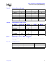
Table 14. Backplane Stripline Stackup
Parameter Routing Guideline Notes
Single Ended Trace Impedance 60 +/- 14% ohms
Differential impedance 100 +/- 15%
Reference Plane ground
Trace Thickness 1.4 mil
Trace Width 11.5 mil
Intra Pair Trace Spacing 29.7 mil intra-pair center-to-center (broadside coupled)
Pair to Pair
Trace Spacing
60 mil
pair-to-pair, center-to-center for two adjacent
differential pairs
Trace Length 2” to 14”
Trace Length Matching 10 mils intra-pair matching
R1 15 +/- 5% ohms
Required only for the write topology shown in
Figure 13.
R2 150 +/- 5% ohms
Required only for the write topology shown in
Figure 13.
Figure 16. Stripline Stackup
B0425-01
1.4 mil
1
.4 mil
49.5 mil
11.5 mil
Er = 4.66
Er = 4.66
Er = 4.66
29.7 mil
17 mil
+ ++
– ––
1.4 mil


