50 Design Guide
Intel
®
31244 PCI-X to Serial ATA Controller
PCI-X Layout Guidelines
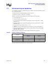
7.4 PCI-X Layout Guidelines For Slot Configurations
The PCI-X Addendum to the PCI Local Bus Specification, Revision 1.0a recommends the
following guidelines for the number of loads for your PCI-X designs. Any deviation from these
maximum values requires close attention to layout with regard to loading and trace lengths.
The following PCI-X design layout considerations were compiled from the white paper Design,
Modeling and Simulation Methodology for High Frequency PCI-X Subsystems available on the
http://www.pcisig.com website.
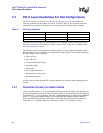
The following results were compiled from the simulation of system models that included system
board and add-in cards for different slot configurations and bus speeds. This simulation addressed
the signal integrity issues including:
• reflective noise
• cross-talk noise
• overshoot/undershoot voltage
• ring-back voltage
• settling time
• inter-symbol interference
• input reference voltage offset
• ground bounce effects
All these results met the required PCI-X timing characteristics and were within appropriate noise
margins.
7.4.1 Protection Circuitry for Add-in Cards
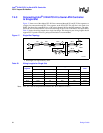
Add-in cards designed for 3.3 V may still need to provide protection circuitry on the interrupt lines
to prevent damaging the GD31244. This is important in the case where the GD31244-based add-in
card (biased to 3.3 V), may potentially plug into a motherboard that has its interrupt lines (INTA#)
tied to 5 V. To prevent potential damage, it is recommended that Schottky diodes be added to
protect the GD31244 input buffer. The anode is connected to the INTA# pin and the cathode is
connected to 3.3 V. Schottky diodes are used because of the 0.3 V forward bias voltage.
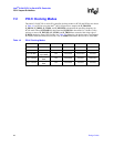
Table 21. PCI-X Slot Guidelines
Frequency Maximum Loads Maximum Number of Slots
66 MHz 8 4
100 MHz 4 2
133 MHz 2 1


