


26 Intel® 41210 Serial to Parallel PCI Bridge Design Guide
General Routing Guidelines
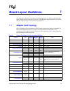
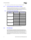
• Avoid slots in the ground plane. Slots increases mutual inductance thus increasing crosstalk.
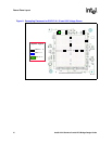
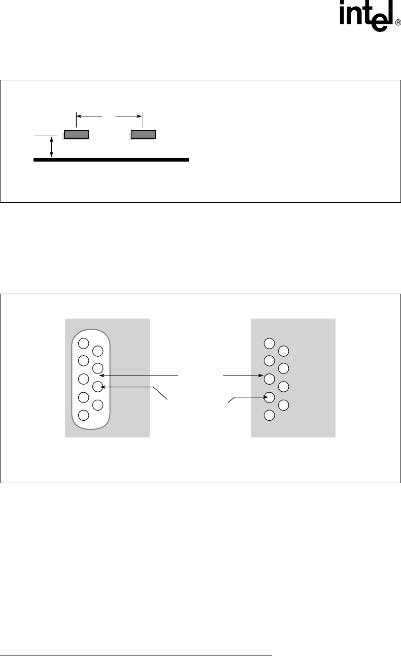
• Make sure that ground plane surrounding connector pin fields are not completely cleared out.
When this area is completely cleared out, around the connector pins, all the return current must
flow together around the pin field increasing crosstalk. The preferred method of laying out a
connector in the GND layer is shown in Figure 12.
6.3 EMI Considerations
It is highly recommended that good EMI design practices be followed when designing with the
41210 Bridge.
• To minimize EMI on your PCB a useful technique is to not extend the power planes to the
edge of the board.
• Another technique is to surround the perimeter of your PCB layers with a GND trace. This
helps to shield the PCB with grounds minimizing radiation.
The below link can provide some useful general EMI guidelines considerations:
http://developer.intel.com/design/auto/mcs96/applnots/272673.htm
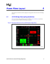
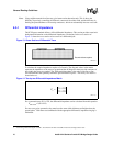
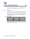
Figure 11. Crosstalk Effects on Trace Distance and Height
A9259-01
Reference Plane
P
aggressor victim
H
Reduce Crosstalk:
- Maximize P
- Minimize H
Figure 12. PCB Ground Layout Around Connectors
A9260-01
A. Incorrect method B. Correct method
Connector
GND PCB Layer
Connector Pins