


iv Intel® 41210 Serial to Parallel PCI Bridge Design Guide
Contents
8.6.1 Embedded PCI-X 133 MHz ...................................................................................39
8.6.2 Embedded PCI-X 100 MHz ...................................................................................40
8.6.3 PCI-X 66 MHz Embedded Topology......................................................................41
8.6.4 PCI 66 MHz Embedded Topology .........................................................................42
8.6.5 PCI 33 MHz Embedded Mode Topology ...............................................................43
9 PCI Express Layout.....................................................................................................................45
9.1 General recommendations .................................................................................................45
9.2 PCI-Express Layout Guidelines..........................................................................................46
9.3 Adapter Card Layout Guidelines.........................................................................................46
10 Circuit Implementations..............................................................................................................49
10.1 41210 Bridge Analog Voltage Filters ..................................................................................49
10.1.1 PCI Analog Voltage Filters.....................................................................................50
10.1.2 PCI Express Analog Voltage Filter ........................................................................50
10.1.3 Bandgap Analog Voltage Filter..............................................................................51
10.2 Intel® 41210 Serial to Parallel PCI Bridge Reference and Compensation Pins.................53
10.2.1 SM Bus ..................................................................................................................54
11 41210 Bridge Customer Reference Boards...............................................................................55
11.1 Board Stack-up...................................................................................................................55
11.2 Material...............................................................................................................................56
11.3 Impedance..........................................................................................................................56
11.4 Board Outline......................................................................................................................57
12 Design Guide Checklist ..............................................................................................................59
Figures
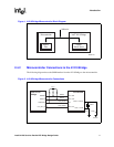
1 41210 Bridge Microcontroller Block Diagram .............................................................................11
2 41210 Bridge Microcontroller Connections.................................................................................11
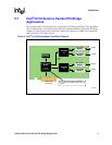
3 41210 Bridge Block Diagram......................................................................................................12
4Intel
®
41210 Bridge Adapter Card Block Diagram......................................................................13
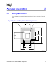
5 Top View - 41210 Bridge 567-Ball FCBGA Package Dimensions..............................................15
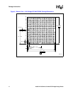
6 Bottom View - 41210 Bridge 567-Ball FCBGA Package Dimensions ........................................16
7 Side View - 41210 Bridge 567-Ball FCBGA Package Dimensions.............................................17
8 Decoupling Placement for Core and PCI Express Voltage Planes ............................................19
9 Decoupling Placement for PCI/PCI-X 1.5V and 3.3V Voltage Planes........................................20
10 41210 Bridge Single-Layer Split Voltage Plane..........................................................................22
11 Crosstalk Effects on Trace Distance and Height ........................................................................26
12 PCB Ground Layout Around Connectors ................................................................................... 26
13 Cross Section of Differential Trace.............................................................................................28
14 Two-by-two Differential Impedance Matrix .................................................................................28
15 Adapter Card Stackup ................................................................................................................30
16 PCI RCOMP ............................................................................................................................... 33
17 PCI Clock Distribution and Matching Requirements...................................................................36
18 Embedded PCI-X 133 MHz Topology ........................................................................................39
19 Embedded PCI-X 100 MHz Topology ........................................................................................40
20 PCI-X 66 MHz Embedded Routing Topology .............................................................................41
21 PCI 66 MHz Embedded Topology ..............................................................................................42