


62 Intel® 41210 Serial to Parallel PCI Bridge Design Guide
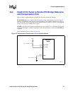
Design Guide Checklist
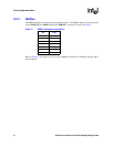
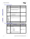
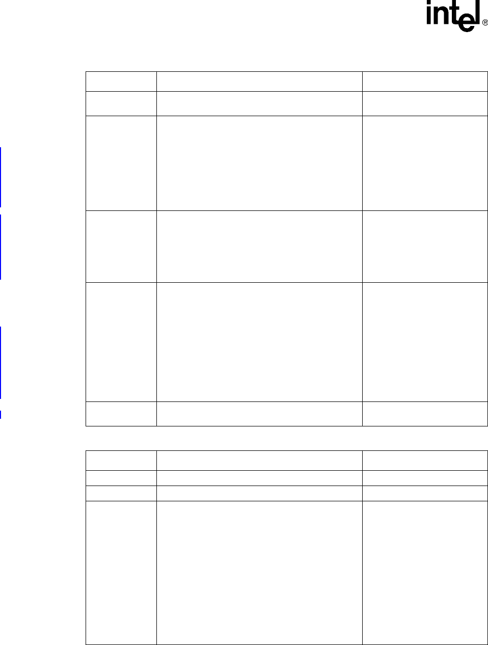
Table 21. Miscellaneous Signals
Signals Recommendations Reason/Impact
RSTIN#
Used for debug purposes. Connect to VCC33 through
an 8.2KΩ pullup resistor for normal operation.
A_STRAP0,
A_STRAP1,
A_STRAP2,
A_STRAP6,
B_STRAP0,
B_STRAP1,
B_STRAP2,
B_STRAP6
RESERVED [8:1]
These signals REQUIRE external pull-downs to GND
on the board 8.2KΩ unless otherwise stated.
CFGRETRY
Input pin to configure 41210 to retry configuration
accesses on it's PCI Express interface.
• To retry configuration accesses to the 41210, pull high to
3.3V through a 2K
Ω resistor.
• To allow configuration accesses to the 41210, ground this
pin through a 2K Ω resistor.
A_TEST1,
A_TEST2,
B_TEST1,
B_TEST2
A_PME#,
B_PME#,
A_STRAP[3],
A_STRAP[4],
A_STRAP[5],
B_STRAP[3],
B_STRAP[4],
B_STRAP[5]
These signals REQUIRE an external pull-up, 8.2KΩ to
3.3V.
NC17 This signal requires an external pull-up, 8.2KΩ to 3.3V.
In normal operating mode, this
pin must be tied high.
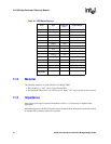
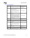
Table 22. SMBus Interface Signals
Signal Recommendations Reason/Impact
SMBCLK Connect to VCC33 through an 8.2KΩ pullup resistor.
SMBDAT Connect to VCC33 through an 8.2KΩ pullup resistor.
SMBUS[5],
SMBUS[3:1]
SMBus addressing:
Bit 7----------------’1’
Bit 6----------------’1’
Bit 5---------------SMBUS[5]
Bit 4----------------’0’
Bit 3---------------SMBUS[3]
Bit 2---------------SMBUS[2]
Bit 1---------------SMBUS[1]
Use 8.2KΩ resistors as pullups to VCC33 for a ‘1’ and
as pulldowns to ground for a ‘0’ to set the SMBus
address.
Sampled on the rising edge of
PERST#.