


Intel® 41210 Serial to Parallel PCI Bridge Design Guide 63
Design Guide Checklist
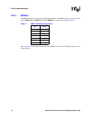
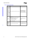
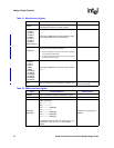
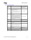
Table 23. Power and Ground Signals
Signal Recommendations Reason/Impact
RCOMP
100Ω ±1% (1/4 W) pulldown resistor to ground.
The trace impedance of this signal should be < 0.1Ω.
Analog compensation pin for
PCI. 0.75V nominal.
VCC15
Connect to 1.5V power supply.
Note: Linear voltage regulators are recommended
when using 1.5 Volt power supplies.
Decoupling:
5 0.1uF caps beneath package (backside of board)
2 1.0 uF caps as close as design rules permit to
package
3 10 uF caps as close as design rules permit to
package
1.5V ±5% core voltage.
VCC33
Connect to 3.3V power supply.
Decoupling: TBD
The platform must insure that the VCC33 voltage rail
be greater than to (or no less than 0.5V below) VCC15
(absolute voltage value at all times during 41210
Bridge operation, including during system power up,
power down or any other time during system operation.
This can be accomplished by placing a diode (with a
voltage drop < 0.5V) between VCC15 and VCC33.
Anode will be connected to VCC15 and cathode will be
connected to VCC33.
3.3V ±5% PCI I/O voltage.
VCCAPE
Connect to 1.5V power supply.
1.5V ±3% Analog PCI Express
voltage.
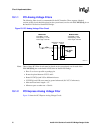
VCCAPCI[2:0] See Figure 23 for circuit. Analog PCI voltage pins.
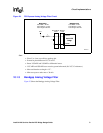
VCCBGPE
Voltage output of the bandgap filter circuit into 41210
Bridge, separated from the rest of the VCC15s. See
Figure 25 for circuit.
2.5V ±3% PCI Express voltage.
VCCPE
Connect to 1.5V power supply.
Decoupling:
3 0.1uF caps beneath package (backside of board)
4 1.0 uF caps as close as design rules permit to
package
2 10 uF caps as close as design rules permit to
package
1.5V ±3% PCI Express voltage.
VSS Connect to ground.
Ground reference for all
supplies.
VSSAPE See Figure 24 for circuit. Analog ground for PCI Express.
VSSBGPE
Ground for the bandgap filter circuit, separated from
the rest of the VSSs. See Figure 25 for circuit.
Ground for analog bandgap
voltage.