


Intel® 41210 Serial to Parallel PCI Bridge Design Guide 35
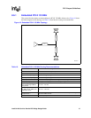
PCI-X Layout Guidelines
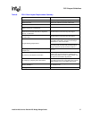
B_CBE#[7:4], B_DEVSEL#, B_FRAME#, B_INTA#, B_INTB#, B_INTC#, B_INTD#,
B_IRDY#, B_PERR#, B_PAR, B_GNT#[5:0], B_REQ#[5:0], B_LOCK#, B_PAR64, B_REQ64#,
B_SERR#, B_STOP#, and B_TRDY#.
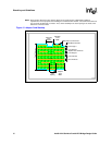
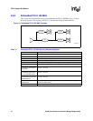
8.4 PCI Clock Layout Guidelines
The PCI-X Addendum to the PCI Local Bus Specification, Revision 1.0b compliant, allows a
maximum of 0.5 ns clock skew timing for each of the PCI-X frequencies: 66 MHz, 100 MHz and
133 MHz. A typical PCI-X application may require separate clock point-to-point connections
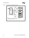
distributed to each PCI device. The 41210 Bridge provides seven buffered clocks on the PCI bus to
connect to multiple PCI-X devices. The Figure 17 shows the use of four PCI “A” clock outputs and
length matching requirements. These same guidelines apply to the 41210 Bridge PCI “B” clock
outputs. The recommended clock buffer layout are specified as follows:
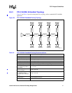
• Match each of the used the 41210 Bridge output clock lengths A_CLK[6:0] and B_CLK[6:0]
to within 0.1” to help keep the timing within the 0.5 ns maximum budget.
• Keep the distance between the clock lines and other signals “d” at least 25 mils from each other.
• Keep the distance between the clock line and itself “a” at a minimum of 25 mils apart (for
serpentine clock layout).
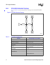
• A_CLKIN gets connected to A_CLKO6 through a 22Ω +/- 1% resistor and likewise for
B_CLKIN is connected to B_CLKO6 through a 22
Ω resistor.
• The 22 +/- 1% Ω resistor is within 500 mils of A_CLKO.