


50 Intel® 41210 Serial to Parallel PCI Bridge Design Guide
Circuit Implementations
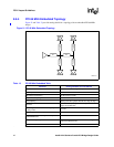
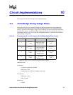
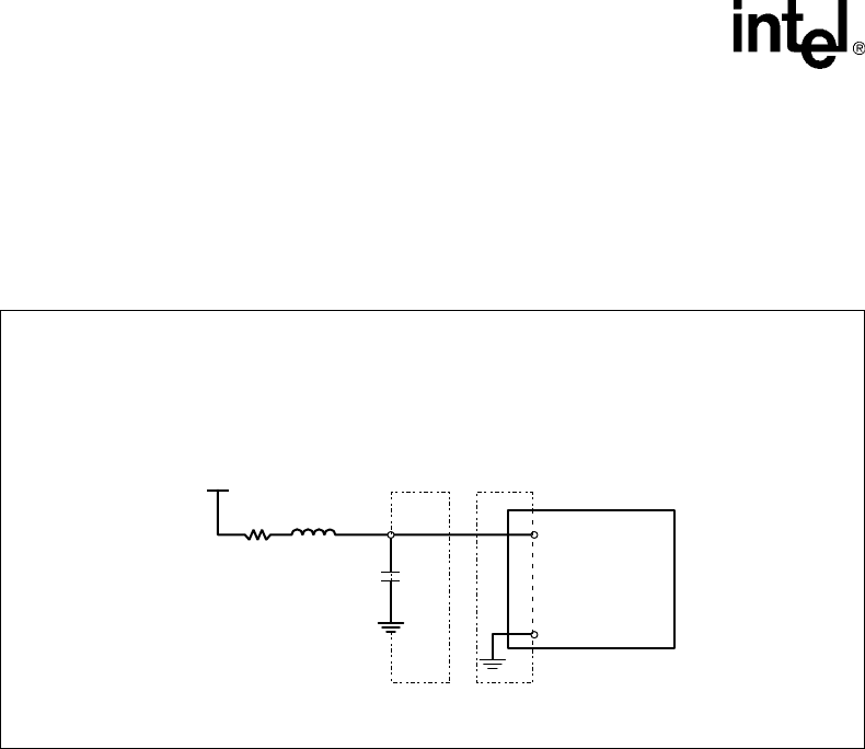
10.1.1 PCI Analog Voltage Filters
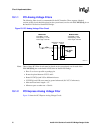
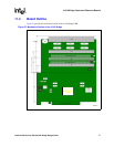
The following filter circuit is recommended for the PCI interface. Three separate, identical
versions of this circuit should be placed on the system board, one for each VCCAPCI[2:0] pin on
the Intel® 41210 Serial to Parallel PCI Bridge.
Figure 23. PCI Analog Voltage Filter Circuit
Note: Three of these PCI filter circuits must be placed on the system board, one for each of the
VCCAPCI[2:0] pins on the Intel® 41210 Serial to Parallel PCI Bridge.
• Place C as close as possible to package pin.
• R must be placed between VCC15 and L.
• Route VCCPCI[x] and VSS as differential traces.
• VCCPCI[x] and VSS traces must be ground referenced (No VCC15 references).
• Max total board trace length = 1.2”.
• Min trace space to other nets = 30 mils.
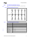
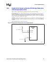
10.1.2 PCI Express Analog Voltage Filter
Figure 24 shows the PCI Express Analog Voltage Circuit.
B2724 -01
R
C
VSS
Intel
fi
41210
Bridge
VCCAPCI[2:0]
L
VCC
Board Trace:
Trace Width > 25 mils
Trace Spacing < 10 mils
Trace Length < 600 mils
Breakout Trace:
Trace Width > 6 mils
Trace Spacing < 6 mils
Trace Length < 600 mils
Board Route
Traces
Breakout
Traces