


Intel® 41210 Serial to Parallel PCI Bridge Design Guide iii
Contents
Contents
1 About This Document ...................................................................................................................7
1.1 Terminology and Definitions .................................................................................................7
2 Introduction....................................................................................................................................9
2.1 PCI Express Interface Features............................................................................................9
2.2 PCI-X Interface Features ......................................................................................................9
2.3 Power Management............................................................................................................10
2.4 SMBus Interface .................................................................................................................10
2.4.1 SMBus for configuration register initialization........................................................10
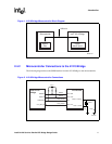
2.4.2 Microcontroller Connections to the 41210 Bridge..................................................11
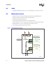
2.5 JTAG...................................................................................................................................12
2.6 Related Documents ............................................................................................................12
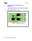
2.7 Intel
®
41210 Serial to Parallel PCI Bridge Applications......................................................13
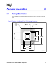
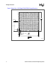
3 Package Information ...................................................................................................................15
3.1 Package Specification ........................................................................................................15
4 Power Plane Layout ....................................................................................................................19
4.1 41210 Bridge Decoupling Guidelines .................................................................................19
4.2 Split Voltage Planes............................................................................................................21
5 41210 Bridge Reset and Power Timing Considerations ..........................................................23
5.1 A_RST#,B_RST# and PERST# Timing Requirements ......................................................23
5.2 VCC15 and VCC33 Voltage Requirements ........................................................................23
6 General Routing Guidelines .......................................................................................................25
6.1 General Routing Guidelines................................................................................................25
6.2 Crosstalk.............................................................................................................................25
6.3 EMI Considerations ............................................................................................................26
6.4 Power Distribution and Decoupling.....................................................................................27
6.4.1 Decoupling.............................................................................................................27
6.5 Trace Impedance................................................................................................................27
6.5.1 Differential Impedance...........................................................................................28
7 Board Layout Guidelines ............................................................................................................29
7.1 Adapter Card Topology.......................................................................................................29
8 PCI-X Layout Guidelines.............................................................................................................31
8.1 Interrupts.............................................................................................................................31
8.1.1 Interrupt Routing for Devices Behind a Bridge.......................................................32
8.2 PCI Arbitration ....................................................................................................................32
8.2.1 PCI Resistor Compensation ..................................................................................33
8.3 PCI General Layout Guidelines ..........................................................................................33
8.3.1 PCI Pullup Resistors Not Required........................................................................34
8.4 PCI Clock Layout Guidelines ..............................................................................................35
8.5 PCI-X Topology Layout Guidelines.....................................................................................38
8.6 Intel
®
41210 Serial to Parallel PCI Bridge Design Guide Layout Analysis .........................38