8 Intel® 41210 Serial to Parallel PCI Bridge Design Guide
About This Document
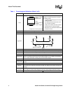
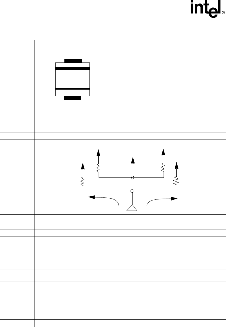
PCB
Printed circuit board.
Example manufacturing process consists of
the following steps:
• Consists of alternating layers of core and
prepreg stacked
• The finished PCB is heated and cured.
• The via holes are drilled
• Plating covers holes and outer surfaces
• Etching removes unwanted copper
• Board is tinned, coated with solder mask
and silk screened
SSTL_2 Series Stub Terminated Logic for 2.5 V
JEDEC Provides standards for the semiconductor industry.
Aggressor
A network that transmits a coupled signal to another network is aggressor network.
Victim A network that receives a coupled cross-talk signal from another network is a victim network.
Network The trace of a PCB that completes an electrical connection between two or more components.
Stub Branch from a trunk terminating at the pad of an agent.
CRB Customer Reference Board
Downstream
Downstream refers either to the relative position of an interconnect/system element (Link/
device) as something that is farther from the Root Complex, or to a direction of information
flow, i.e., when information is flowing away from the Root Complex.
Upstream
Local memory
Memory subsystem on the Intel XScale
®
core DDR SDRAM or Peripheral Bus Interface
busses.
DWORD 32-bit data word.
Flip Chip
FC-BGA (flip chip-ball grid array) chip packages are designed with processor core flipped up
on the back of the chip, facing away from the PCB. This allows more efficient cooling of the
package.
Mode
Conversion
Mode Conversions are due to imperfections on the interconnect which transform differential
mode voltage to common mode voltage and common mode voltage to differential voltage.
PCI-E PCI-Express
Table 1. Terminology and Definitions (Sheet 2 of 2)
Term Definition
Layer 1: copper
Prepreg
Layer 2: GND
Core
Layer 3: VCC15
Layer 4: copper
Prepreg
Example of a Four-Layer Stack
Aggressor Network
Victim Network
Zo
Zo
Zo
Zo


