


Intel® Server Board SE7320SP2 & Intel Server Board SE7525GP2 TPS Functional Architecture
Revision 2.0
38
3.5 Memory Sub-System
On the Intel Server Board SE7320SP2 and Intel Server Board SE7525GP2, the MCH provides
an integrated memory controller for direct connection to two channels of registered DDR266 or
DDR333 memory (stacked or unstacked). Peak theoretical memory data bandwidth using
DDR266 technology is 4.26 GB/s and 5.33 GB/s for DDR333 technology.
When both DDR channels are populated and operating, they function in lock-step mode. The
maximum supported memory size for either memory speed is 8GB.
The MCH supports a burst length of four whether in single or dual channel mode. In dual
channel mode this results in eight 64-bit chunks (64-byte cache line) from a single read or write.
In single channel mode two reads or writes are required to access a cache line of data.
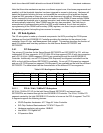
3.5.1 Memory Sizing
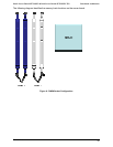
Both the Intel Server Board SE7320SP2 and Intel Server Board SE7525GP2 provide four
DDR266 / DDR333 DIMM sites. There are two DIMM sites on each memory channel.
DIMMs on channel A are paired with DIMMs on channel B to configure 2-way interleaving. The
minimum memory configuration to support interleaving is two DIMMs, which requires same
DIMM populated from each channel. Each board does support single channel memory
operation with a single DIMM populated in DIMM location 1 on either bank (1A or 2A). It should
be noted that single channel operation greatly reduces memory bandwidth and RAS capabilities.
Memory DIMM technologies supported are: 128Mb, 256Mb, 512Mb, 1Gb and 2Gb. Physical
DIMM sizes supported are 256MB, 512MB, 1GB, and 2GB.
Please refer to the Tested Memory List located on the support website for a complete list of
supported memory.
http://support.intel.com/support/motherboards/server/se7320sp2
http://support.intel.com/support/motherboards/server/se7525gp2
The BIOS reads the Serial Presence Detect (SPD) SEEPROMs on each installed memory
module to determine the size and timing of the installed memory modules. The memory sizing
algorithm determines the size of each row of DIMMs. The BIOS programs the Memory
Controller in the chipset accordingly. The total amount of configured memory can be found
using BIOS Setup.
The DIMM pair, which constitutes interleaving, is referred to as a bank. The bank can be further
divided into two rows, based on single-sided or double-sided DIMMs. If both DIMMs in a pair are
single-sided, only one row is said to be present in the system. For double-sided DIMMs, both
rows are said to be present.
For interleaving and RAS to be enabled, memory DIMMs must be populated in pairs. The Intel
Server Board SE7320SP2 and Intel Server Board SE7525GP2 each have four DIMM slots, or
two DIMM banks. Both DIMMs in a bank should be identical (same manufacturer, CAS latency,
number of rows, columns and devices, timing parameters etc.). Although DIMMs within a bank
must be identical, the BIOS supports various DIMM sizes and configurations, allowing the banks
of memory to be different. Memory sizing and configuration is guaranteed only for qualified
DIMMs approved by Intel.