


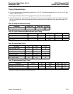
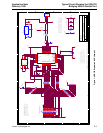
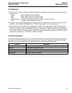
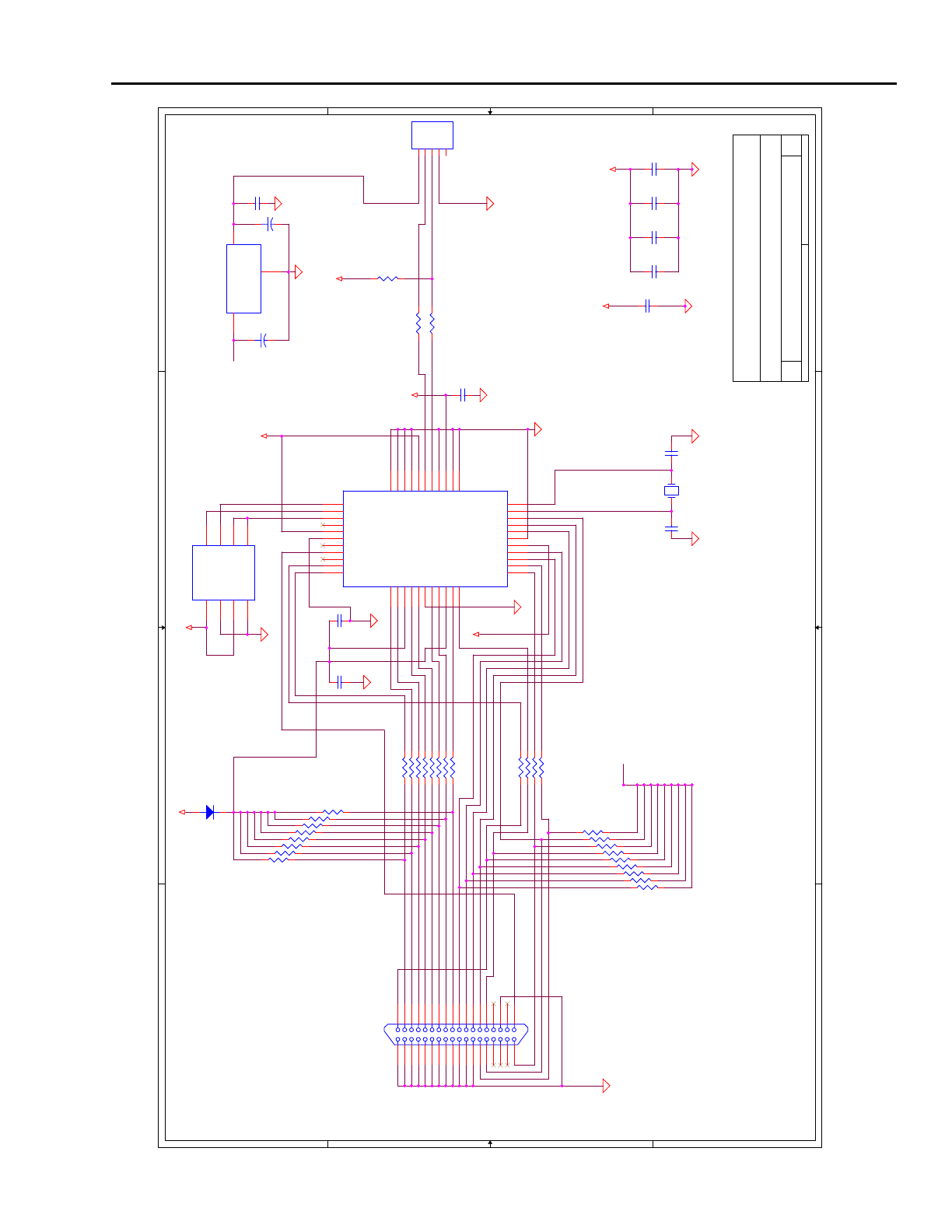
Application Note Typical Circuit Showing the USS-720
February 1999 Bridging USB to Parallel Port
Lucent Technologies Inc. 6-3
13
A
A
B
B
C
C
D
D
4 4
3 3
2 2
1 1
Data_1
PError
SELECT
nFAULT
nACK
nSELECTIN
nFAULT
Data_0
Data_7
BUSY
Data_6
Data_3
Data_0
Data_2
VDD_5V
Data_3
nINIT
nINIT
PLH
Data_5
nSTROBE
PError
Data_7
Data_4
Data_1
BUSY
nSTROBE
Data_6
nSELECTIN
nAUTOFD
PLH
Data_4
SELECT
nACK
Data_5
Data_2
nAUTOFD
VDD_5V
EEPROM
ASIC BYPASS
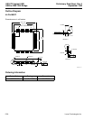
The schematic provided with the
Evaluation Kit is for reference only.
It’s suitability for use for any
particular purpose is not warrented by
Lucent or In-System Design.
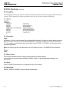
Standard decoupling should be used on the
board. 0.1ufd capacitors between VCC_5V, VCC,
and GND placed as close as possible to the
power pins on the USS-720 is recommended.
Sufficient grounding must be
implemented on the board to ensure
proper functionality. A 4-layer
board design is recommended with
two layers for power and ground
planes.
Copywrite 1997, 1998, In-System Design Inc.
{Doc} B
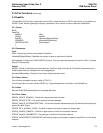
ISD-101 USB to Parallel 1284
In-System Design, Inc.
Boise, Idaho
B
11Wednesday, June 24, 1998
Title
Size Document Number Rev
Date: Sheet
of
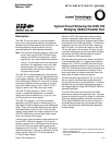
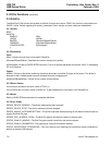
DATA-
DATA+
VCC_5V
GND
VCC5V_pullup
5V_pullup
VCC
VCC
VCC
VCC
VCC_5V
VCC
VCC
VCC
C11
.01ufd
12
C5
.1ufd
12
R12
24
1 2
C7
15 pf
R31
R19
24
1 2
R33
D1
DIODE
R10
1.5k
R28
R27
R2
C6
15 pf
Y1
CRYSTAL
J1
CONNECTOR CENT36
1
2
3
4
5
6
7
8
9
10
11
12
13
14
15
16
17
18
19
20
21
22
23
24
25
26
27
28
29
30
31
32
33
34
35
36
R14
24
1 2
R11
24
1 2
+
C2
3.3ufd tant.
R21
24
1 2
R15
24
1 2
C10
.1ufd
C8
.1ufd
R3
R26R4
R13
24
1 2
R22
24
1 2
R17
24
1 2
R25
+
C1
3.3ufd tant.
R32
R1
R5
C9
.1ufd
R16
24
1 2
R24
24
1 2
R18
24
1 2
C3
.1ufd
R6
R23
24
1 2
R30
R8
R29
U1
LT1121CST_3.3
13
2
VINVOUT
GND
J2
CON5
1
2
3
4
5
RED
WHITE
GREEN
BLACK
SHIELD
R20
24
1 2
C4
.1ufd
C13
.1ufd
U?
93CS56
6
7
5
8 1
2
3
4
nc
nc
GND
VCC CS
SK
DI
DO
C12
.1ufd
U2
QUAD_44_p
34
35
36
37
16
12
38
13
39
26
14
17
15
30
40
41
18
42
19
43
20
44
21
22
29
32
33
23
31
27
28
24
25
1
6
2
3
4
5
7
8
9
10
11
SK
CS
DIO
nUSB_Reset
VCC
nSELECTIN
VCC
nINIT
GND
PLL_VSS
nACK
GND
BUSY
GND
Suspend
PLH
PEerror
HLH
SELECT
nSTROBE
nFAULT
D0
CLK_LO
CLK_HI
VCC
reset
tst_rst
SCAN
test
DPLS
DMNS
SCAN_EN
PLL_VDD
D1
GND
D2
VDD_5V
D3
D4
D5
D6
VDD_5V
D7
nAUTOFD
R7
Figure 1. USS-720 Evaluation Kit Schematic