


Rev.1.10 Jul 01, 2005 page 108 of 318
REJ09B0124-0110
M16C/6N Group (M16C/6NK, M16C/6NM) 12. Timers
Under development
This document is under development and its contents are subject to change.
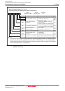
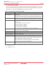
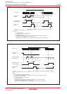
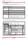
Figure 12.13 Example of 16-bit Pulse Width Modulator Operation
1 / fi ✕ (2
—
1)
16
Count source
Input signal to
TAiIN pin
PWM pulse output
from TAiOUT pin
Trigger is not generated by this signal
"H"
"H"
"L"
"L"
IR bit in TAiIC
register
i = 0 to 4
fj: Frequency of count source (f1, f2, f8, f32, fC32)
"1"
"0"
NOTES:
1. n = 0000h to FFFEh.
2. This timing diagram is the following case.
TAi register = 0003h
The TAiTGH and TAiTGL bits in the ONSF or TRGSR register = 00b (TAiIN pin input)
The MR1 bit in the TAiMR register = 1 (rising edge)
The MR2 bit in the TAiMR register = 1 (trigger selected by the TAiTGH and TAiTGL bits)
1 / fj
✕ n
Set to "0" upon accepting an interrupt request or by writing in program
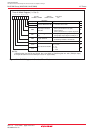
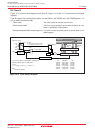
Count source
(1)
Input signal to
TAiIN pin
Underflow signal of
8-bit prescaler
(2)
PWM pulse output
from TAiOUT pin
"H"
"H"
"H"
"L"
"L"
"L"
"1"
"0"
Set to "0" upon accepting an interrupt request or by writing in program
1 / fj ✕ (m
+ 1) ✕ (2
—
1)
8
1 / fj ✕ (m + 1) ✕ n
1 / fj ✕ (m + 1)
IR bit in TAiIC
register
i = 0 to 4
fj: Frequency of count source (f1, f2, f8, f32, fC32)
NOTES:
1. The 8-bit prescaler counts the count source.
2. The 8-bit pulse width modulator counts the output from the 8-bit prescaler underflow signal.
3. m = 00h to FFh; n = 00h to FEh.
4. This timing diagram is the following case.
TAi register = 0202h
The TAiTGH and TAiTGL bits in the ONSF or TRGSR register = 00b (TAiIN pin input)
The MR1 bit in the TAiMR register = 0 (falling edge)
The MR2 bit in the TAiMR register = 1 (trigger selected by the TAiTGH and TAiTGL bits)
Figure 12.14 Example of 8-bit Pulse Width Modulator Operation